Film deposition device

a film deposition and film technology, applied in the direction of electrolysis components, vacuum evaporation coatings, coatings, etc., can solve the problems of insufficient control accuracy, insufficient frequency change, and difficulty in constant so as to achieve accurate measurement and control of film thickness, high response speed

Inactive Publication Date: 2008-04-08
SHIMADZU CORP
View PDF8 Cites 180 Cited by
  • Summary
  • Abstract
  • Description
  • Claims
  • Application Information

AI Technical Summary

Benefits of technology

[0018]In the present invention, it is possible to follow a fluctuation in the plasma quantity at a high response speed in a wide range from a thin film to a thick film. Accordingly, it is possible to accurately measure and control a film thickness.

Problems solved by technology

In the structures, a control area and control accuracy of the film thickness are not sufficient.
However, in the time control, there is no function to follow the fluctuation, i.e. a change in the film deposition rate, in real time, thereby making it difficult to constantly control the film thickness.
The frequency change is generally not large enough for measuring a thin film having a thickness less than 100 nm.
Accordingly, when a protective film having a thickness of, for example, 2 to 3 nm, is formed on a magnetic head, it is difficult to use the method.
However, it is necessary to take time for analysis to measure the polarization quantity and calculate a thickness.
In particular, when a film has a thickness less than several tens of nm, the film deposition time becomes shorter than the analysis time, so that it is very difficult to accurately control a film thickness.
Therefore, in order to apply the method with high precision, it is necessary to reduce the film deposition rate to an extremely small rate, or interrupt the film deposition several times to measure a film thickness repeatedly, thereby making the process complicated and lowering throughput.
Further, in the system shown in FIG. 7, when a distribution of the plasma flow 3 entering the depositing chamber 6 through the guiding path 2 is fluctuated with time, the correlation between the output of the monitoring sensor 7 and a thickness of a film deposited on the substrate 10 is impaired, thereby making it difficult to accurately control a film thickness.

Method used


Image

  • Film deposition device
  • Film deposition device
  • Film deposition device

Examples


Embodiment Construction

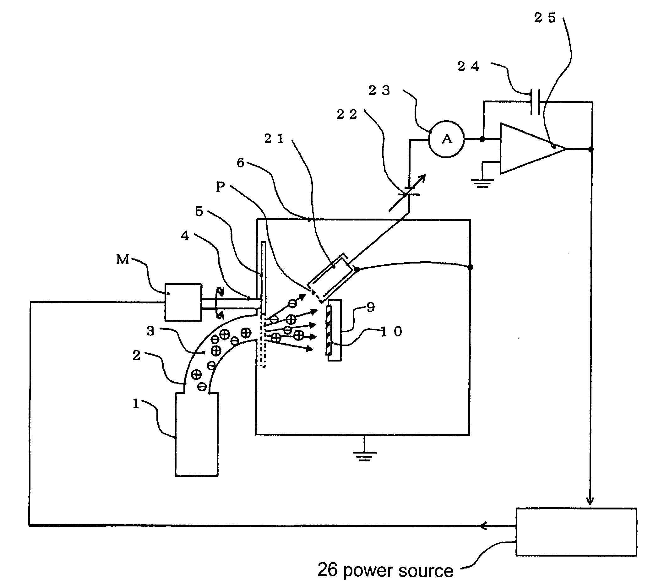
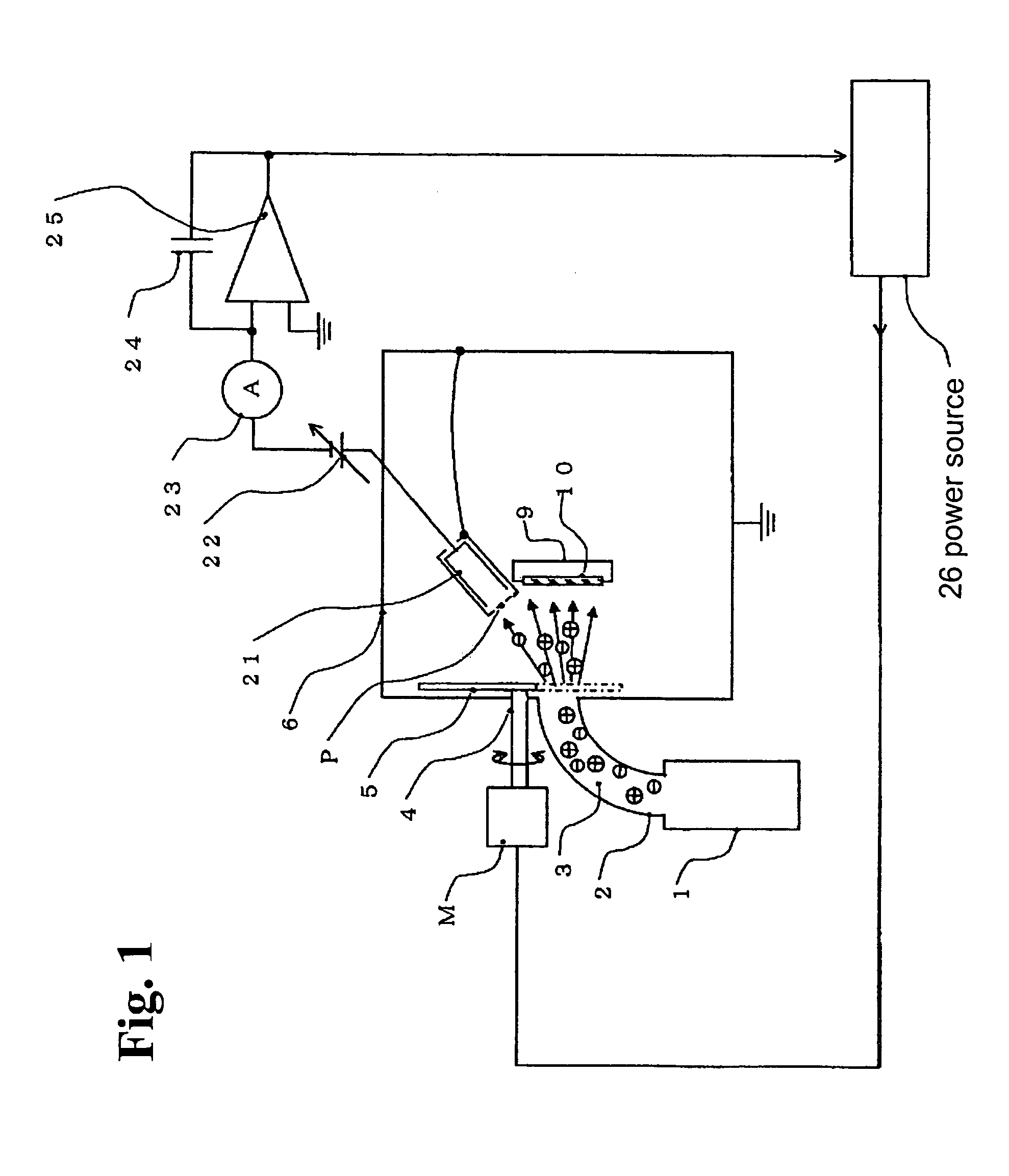
[0027]Hereunder, embodiments of the present invention will be explained with reference to the accompanying drawings. A film deposition device has a film deposition chamber, or a depositing chamber, for generating plasma of a material to be deposited to form a film. A plasma quantity monitoring device is disposed in the depositing chamber for monitoring a plasma quantity at real time, and a calculating device is provided for calculating a thickness of a deposit or film, so that the thickness of the deposit or film is monitored at real time. A quantity of electrons constituting the plasma is measured to monitor the plasma quantity. Incidentally, in the following embodiments, the plasma quantity monitoring device is called a Faraday cup.

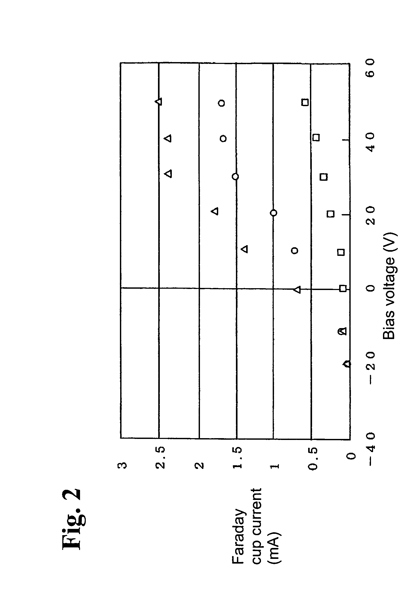
[0028]FIG. 1 is a block diagram showing a structure according to an embodiment of the present invention. Reference numeral 1 represents a plasma source for generating a plasma flow 3, i.e. a mixture of positive ions of a material to be deposited and ele...


PUM

PropertyMeasurementUnit
thicknessaaaaaaaaaa
thicknessaaaaaaaaaa
thicknessaaaaaaaaaa

Abstract

A film deposition device for depositing a film includes a depositing chamber for depositing the film with plasma. A plasma quantity monitoring device is disposed in the depositing chamber for monitoring a plasma quantity entering the depositing chamber at real time. A calculating device is electrically connected to the plasma quantity monitoring device for calculating a thickness of the film from the plasma quantity so that the thickness is monitored at real time.

Description

BACKGROUND OF THE INVENTION AND RELATED ART STATEMENT[0001]The invention relates to a film deposition device for depositing a protective film or a functional film on a surface of a film material such as a film and sheet, or a solid material such as a magnetic head.[0002]Heretofore, in order to control a thickness of a film deposited by a film deposition device and stop the device at appropriate time, a time control or in-situ film thickness monitoring control has been carried out. In the time control, it is assumed that a film thickness is proportional to film deposition time. The film thickness and the film deposition time are measured beforehand, and a film deposition speed per unit time is calculated. The film deposition is stopped manually or automatically at time when a desired thickness is obtained based on the data obtained described above. In the in-situ film thickness monitoring control, a thickness is measured at real time by using a quartz oscillator type film thickness m...

Claims


Application Information

Patent Timeline
Patent Type & Authority Patents(United States)
IPC IPC(8): H01L21/00C23C14/00C23C16/00C23C14/54C23C16/52H01J37/32
CPCC23C14/544C23C16/52H01J37/32935
Inventor KONISHI, YOSHIYUKIOSANAI, KATSUTOYO
Owner SHIMADZU CORP
Why Eureka
Try Eureka