Method for programming non-volatile memory with reduced program disturb using modified pass voltages

a non-volatile memory and program disturb technology, applied in static storage, digital storage, instruments, etc., can solve the problems of band-to-band tunneling or gate-induced drain leakage (gidl) related breakdown, inability of conventional channel boosting techniques to reduce program disturb, and inability to sufficiently isolate the channel length of memory elements, etc., to achieve the effect of reducing the leakage of charge and boosting the potential of associated channel regions

Active Publication Date: 2008-04-08
SANDISK TECH LLC
View PDF48 Cites 63 Cited by
  • Summary
  • Abstract
  • Description
  • Claims
  • Application Information

AI Technical Summary

Benefits of technology

[0014]In one embodiment, a method for programming non-volatile storage includes programming a selected non-volatile storage element in a set of non-volatile storage elements by applying a programming voltage on a selected word line. Additionally, during the programming, a higher pass voltage is applied to word lines associated with previously programmed non-volatile storage elements than to word lines associated with unprogrammed and / or partly programmed non-volatile storage elements. The pass voltages boost a potential of associated channel regions. In particular, the potential of the channel region associated with the previously programmed non-volatile storage elements is approximately balanced with the potential of the channel region associated with the unprogrammed and / or partly programmed non-volatile storage elements. As a result, the differential in the pass voltages reduces the leakage of charge from the channel region associated with the unprogrammed and / or partly programmed non-volatile storage elements to the channel region associated with the previously programmed non-volatile storage elements. Depending on the implementation, the differential in the pass voltages can be approximately two to three volts. Moreover, when the set of non-volatile storage elements is programmed starting at a source side and ending at a drain side, a higher pass voltage is applied to the source side word lines than to the drain side word lines.

Problems solved by technology

However, with ever decreasing channel lengths in memory elements, e.g., 90 nm or less, the ability of conventional channel boosting techniques to reduce program disturb is compromised.
In particular, the channel length of the memory elements can become too short to sufficiently isolate the two separately boosted channel areas at the drain and source sides of the selected word line.
Additionally, band-to-band tunneling or gate induced drain leakage (GIDL) related breakdown can occur near the drain of the grounded word line.
Due to this breakdown, the boosted channel can be discharged, causing program disturb, and / or hot carriers may be generated that are injected in the tunnel oxides or into the floating gates of the memory cells.

Method used


Image

  • Method for programming non-volatile memory with reduced program disturb using modified pass voltages
  • Method for programming non-volatile memory with reduced program disturb using modified pass voltages
  • Method for programming non-volatile memory with reduced program disturb using modified pass voltages

Examples


Embodiment Construction

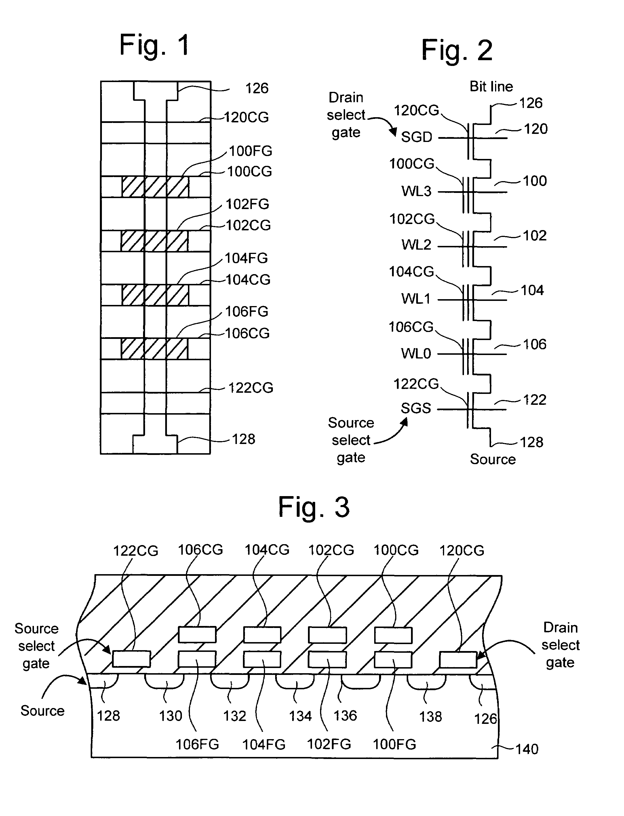
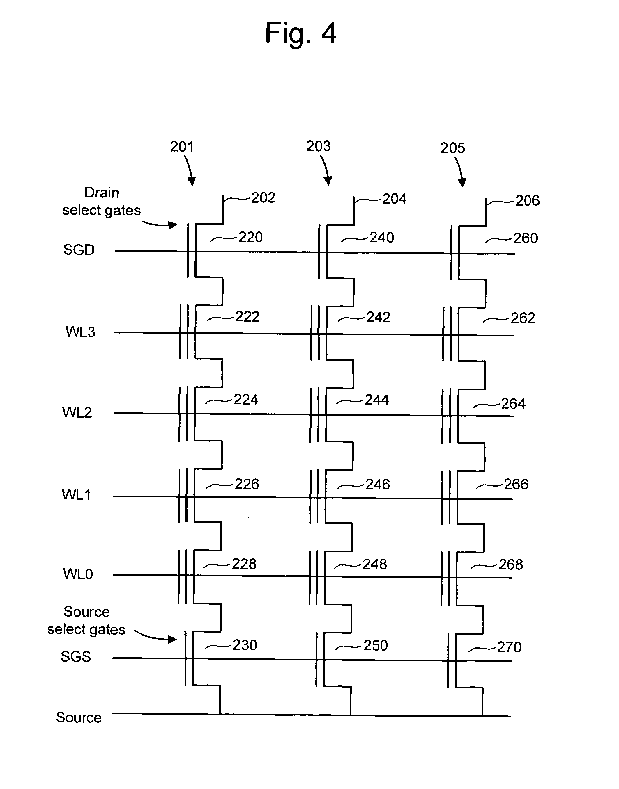
[0030]One example of a non-volatile memory system suitable for implementing the present invention uses the NAND flash memory structure, in which multiple transistors are arranged in series between two select gates in a NAND string. FIG. 1 is a top view showing one NAND string. FIG. 2 is an equivalent circuit thereof. The NAND string depicted in FIGS. 1 and 2 includes four transistors, 100, 102, 104 and 106, in series and sandwiched between a first select gate 120 and a second select gate 122. Select gates 120 and 122 connect the NAND string to bit line contact 126 and source line contact 128, respectively. Select gates 120 and 122 are controlled by applying the appropriate voltages to control gates 120CG and 122CG, respectively. Each of the transistors 100, 102, 104 and 106 has a control gate and a floating gate. Transistor 100 has control gate 100CG and floating gate 100FG. Transistor 102 includes control gate 102CG and floating gate 102FG. Transistor 104 includes control gate 104C...


PUM


Abstract

Non-volatile storage elements are programmed in a manner that reduces program disturb by using modified pass voltages. In particular, during the programming of a selected storage element associated with a selected word line, a higher pass voltage is applied to word lines associated with previously programmed non-volatile storage elements in the set than to word lines associated with unprogrammed and / or partly programmed non-volatile storage elements in the set. The pass voltage is sufficiently high to balance the channel potentials on the source and drain sides of the selected word line and / or to reduce leakage of charge between the boosted channel regions. Optionally, an isolation region is formed between the boosted channel regions by applying a reduced voltage on one or more word lines between the selected word line and the word lines that receive the higher pass voltage.

Description

CROSS-REFERENCE TO RELATED APPLICATIONS[0001]This application is related to U.S. patent application Ser. No. 10 / 774,014, published as 2005 / 0174852 on Aug. 11, 2005, titled “Self-boosting system for flash memory cells”, and incorporated herein by reference.BACKGROUND OF THE INVENTION[0002]1. Field of the Invention[0003]The present invention relates to programming non-volatile memory with reduced program disturb.[0004]2. Description of the Related Art[0005]Semiconductor memory has become increasingly popular for use in various electronic devices. For example, non-volatile semiconductor memory is used in cellular telephones, digital cameras, personal digital assistants, mobile computing devices, non-mobile computing devices and other devices. Electrically Erasable Programmable Read Only Memory (EEPROM) and flash memory are among the most popular non-volatile semiconductor memories. With flash memory, also a type of EEPROM, the contents of the whole memory array, or of a portion of the ...

Claims


Application Information

Patent Timeline
Patent Type & Authority Patents(United States)
IPC IPC(8): G11C11/34
CPCG11C11/5628G11C16/0483G11C16/12G11C16/3418G11C16/3427G11C16/3459G11C2211/5621
Inventor HEMINK, GERRIT JANOOWADA, KEN
Owner SANDISK TECH LLC
Why Eureka
Try Eureka