Semiconductor memory device and method for writing to semiconductor memory device

a memory device and semiconductor technology, applied in static storage, digital storage, instruments, etc., can solve the problems of increasing the chip area, writing cannot, and the current supply capacity of the internal pumping circuit is limited, so as to reduce the area of the pumping capacitor of the internal pumping circuit, suppress the excess increase of source potential upon programming, and reduce the leakage current flowing in the bit line.

Active Publication Date: 2008-04-08
FUJITSU LTD
View PDF17 Cites 5 Cited by
  • Summary
  • Abstract
  • Description
  • Claims
  • Application Information

AI Technical Summary

Benefits of technology

[0020]The high voltage to be applied upon the writing is generated by the internal pumping circuit, and the current-supplying capacity of the internal pumping circuit is limited by the size of the pumping capacitor of the pumping circuit, etc. If the current-supplying capacity of the pumping circuit is below a current following through the bit line, a voltage to be applied to the bit line upon the writing is dropped, and when the drop is large, the writing cannot be made. The problem of such the voltage decrease can be prevented by increasing the current-supplying capacity of the pumping circuit, and in such case, the pumping capacitor must be increased. This increases the chip area, and the electric power consumption for the writing is increased too.
[0022]An object of the present invention is to provide a structure of a semiconductor memory device which can decrease the leakage current flowing in the bit lines upon the writing while suppressing increases of the chip area, and a method for writing to the semiconductor memory device.
[0025]According to the present invention, the write-back programming is executed by connecting the internal pumping circuit supplying a negative voltage to the side of the source line of the n-channel memory cell transistors and applying the prescribed voltages to the other terminals with reference to the voltage of the source terminal as the reference voltage, whereby even when the currents flowing in the bit lines are large, and the source potential is increased, the leakage current can be automatically suppressed by the source potential increase, and the excessive increase of the source potential upon the programming can be suppressed. Thus, the leakage currents flowing in the bit lines upon the programming can be decreased, and the area of the pumping capacitor of the internal pumping circuit can be made small. Accordingly, the chip area of the semiconductor memory device can be reduced, and the electric power consumption for executing the programming can be decreased.

Problems solved by technology

The high voltage to be applied upon the writing is generated by the internal pumping circuit, and the current-supplying capacity of the internal pumping circuit is limited by the size of the pumping capacitor of the pumping circuit, etc.
If the current-supplying capacity of the pumping circuit is below a current following through the bit line, a voltage to be applied to the bit line upon the writing is dropped, and when the drop is large, the writing cannot be made.
This increases the chip area, and the electric power consumption for the writing is increased too.
Since the write-back programming is executed for each bit line which including over erase cells, leakage current of the bit line is usually large and serious.
In the ordinary programming, although no over erase cell is present, the voltage applied to a selected word line is large, which makes the current flowing in the selected cell large, and the balance with the current-supplying capacity of the pumping circuit is an important problem too.

Method used


Image

  • Semiconductor memory device and method for writing to semiconductor memory device
  • Semiconductor memory device and method for writing to semiconductor memory device
  • Semiconductor memory device and method for writing to semiconductor memory device

Examples


first embodiment

A First Embodiment

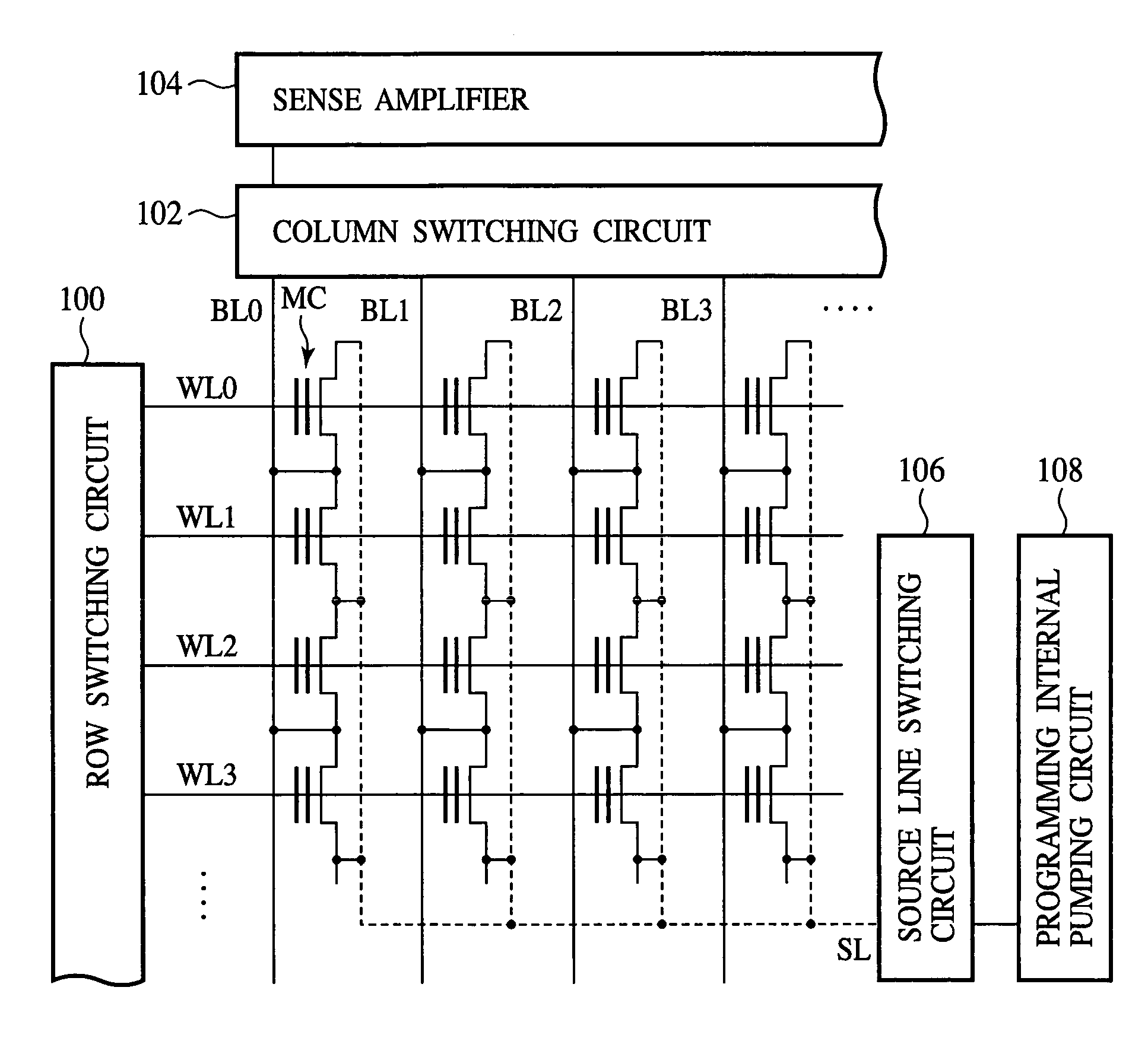
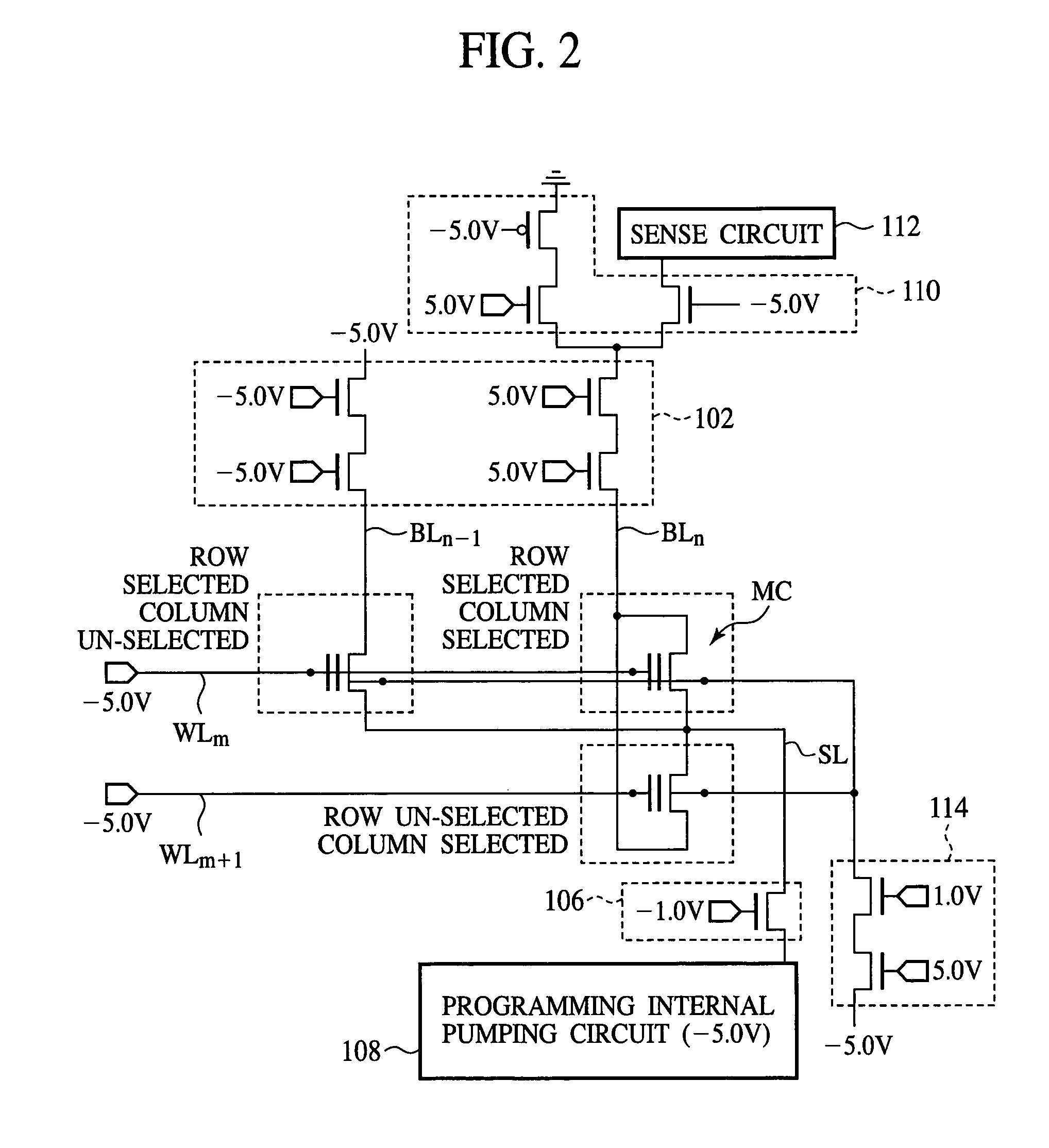
[0044]The semiconductor memory device and method for writing to the semiconductor memory device according to a first embodiment of the present invention will be explained with reference to FIGS. 1 to 5.

[0045]FIG. 1 is a circuit diagram of the semiconductor memory device according to the present embodiment, which shows a structure thereof. FIG. 2 is a circuit diagram showing a method for writing to the semiconductor memory device according to the present embodiment. FIG. 3 is a view showing voltages applied to the respective terminals of the memory cell transistor for the write-back programming of the semiconductor memory device according to the present embodiment. FIG. 4 is a graph showing the transient change of the source potential and the bit line current upon executing the write-back programming. FIG. 5 is a time chart showing the method for writing to the semiconductor memory device according to the present embodiment.

[0046]First, the structure of the semicond...

second embodiment

A Second Embodiment

[0079]The semiconductor memory device and the method for writing to the semiconductor memory device according to the second embodiment of the present invention will be explained with reference to FIG. 6. The same members of the present embodiment as those of the semiconductor memory device and the method for writing to the semiconductor memory device according to the first embodiment shown in FIGS. 1 to 5 are represented by the same reference numbers not to repeat or to simplify their explanation.

[0080]FIG. 6 is a circuit diagram showing a structure of the semiconductor memory device and the method for writing to the semiconductor memory device according to the present embodiment.

[0081]The semiconductor memory device according to the present embodiment is characterized mainly in that, as shown in FIG. 6, an output voltage from the programming internal pumping circuit 108 is applied not only the source line SL, but also to the selected word line (word line WLm) via...

third embodiment

A Third Embodiment

[0088]The semiconductor memory device and the method for writing to the semiconductor memory device according to a third embodiment of the present invention will be explained with reference to FIGS. 7 and 8. The same members of the present embodiment as those of the semiconductor memory device and the method for writing to the semiconductor memory device according to the first and the second embodiments shown in FIGS. 1 to 6 are represented by the same reference numbers not to repeat or to simplify their explanation.

[0089]FIG. 7 is a circuit diagram showing a structure of the semiconductor memory device according to the present embodiment. FIG. 8 is a view showing the structure of the semiconductor memory device and the method for writing to the semiconductor memory device according to the present embodiment.

[0090]The semiconductor memory device according to the present embodiment is characterized mainly in that, as shown in FIG. 7, the source line SL is divided in...


PUM


Abstract

The semiconductor memory device comprising: an n-channel memory cell transistor including: a first diffused region and a second diffused region formed in a semiconductor substrate; a charge storage layer formed over the semiconductor substrate between the first diffused region and the second diffused region; and a gate electrode formed over the charge storage layer; a power supply circuit formed on the semiconductor substrate, the power supply circuit being connectable to the first diffused region, pumping a voltage supplied from an outside power supply and outputting the pumped voltage; and writing means which, upon writing to the n-channel memory cell transistor, applies a reference voltage to the second diffused region, and applies a negative voltage with respective to the reference voltage supplied from the power supply circuit to the first diffused region to thereby flow current between the first diffused region and the second diffused region and to store charges in the charge storage layer.

Description

CROSS-REFERENCE TO RELATED APPLICATIONS[0001]This application is based upon and claims the benefit of priority from the prior Japanese Patent Application No. 2005-037524, filed on Feb. 15, 2005, the entire contents of which are incorporated herein by reference.BACKGROUND OF THE INVENTION[0002]The present invention relates to a semiconductor memory device and a method for writing to the semiconductor memory device, more specifically a semiconductor memory device for memorizing information by storing charges and a method for writing to the semiconductor memory device.[0003]As rewritable nonvolatile semiconductor memory devices are generally known EEPROM, flash EEPROMs, etc., which memorize information by storing charges in the floating gates. For programming in these semiconductor memory devices, charges are injected into the floating gates to thereby write information, and charges stored in the floating gates are extracted to thereby erase information.[0004]The general programming me...

Claims


Application Information

Patent Timeline
Patent Type & Authority Patents(United States)
IPC IPC(8): G11C16/04
CPCG11C16/0416G11C16/12G11C16/3404G11C16/3409G11C16/344G11C16/345
Inventor EMA, TAIJI
Owner FUJITSU LTD
Why Eureka
Try Eureka