Electrochemical cell
a technology of electrochemical cells and cells, applied in the field of electrochemical cells, to achieve the effect of great accuracy and precision
- Summary
- Abstract
- Description
- Claims
- Application Information
AI Technical Summary
Benefits of technology
Problems solved by technology
Method used
Image
Examples
example 1
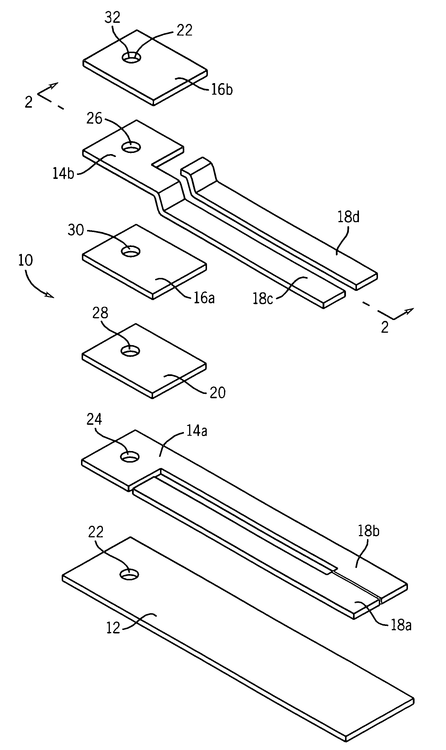
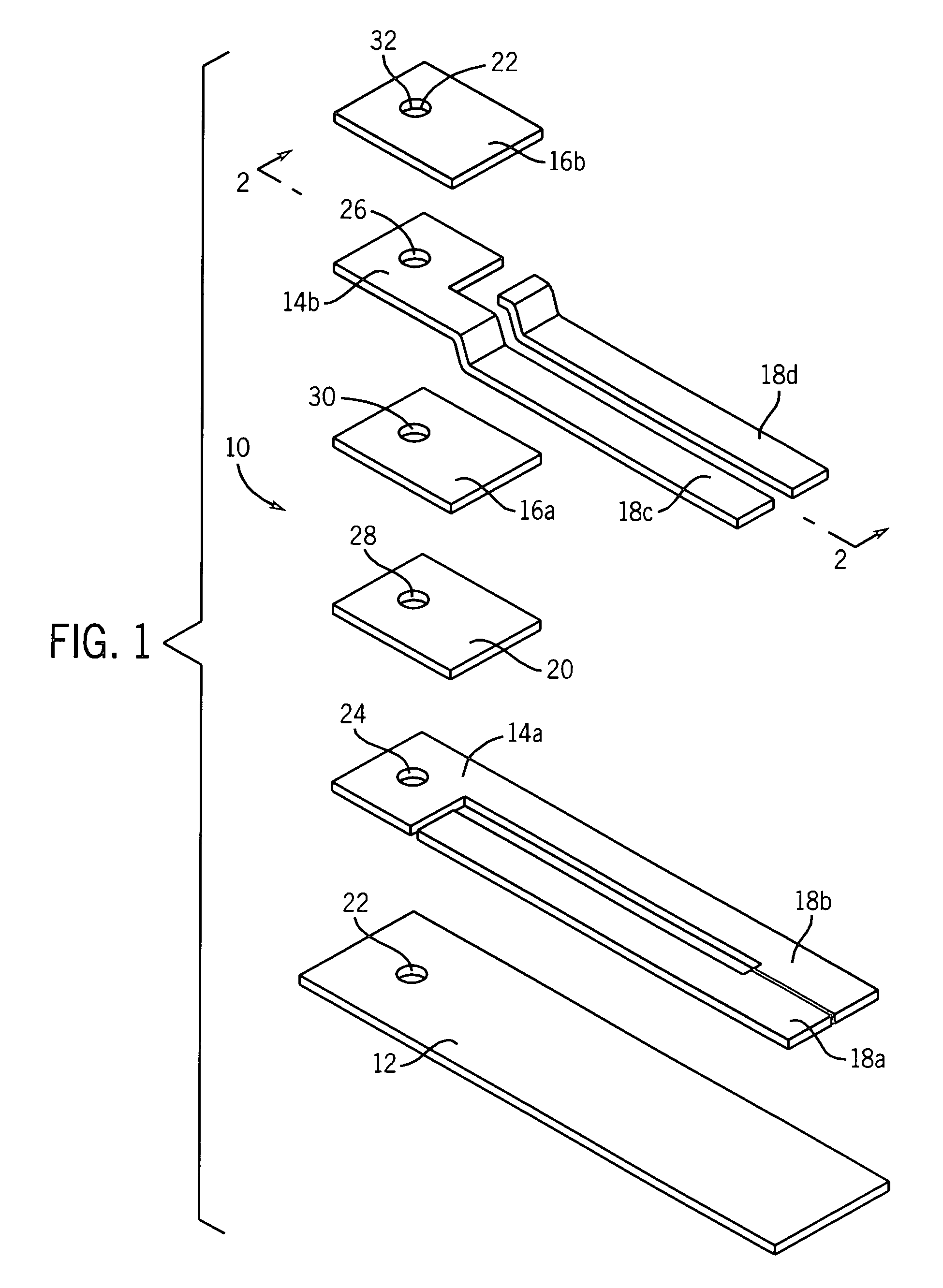
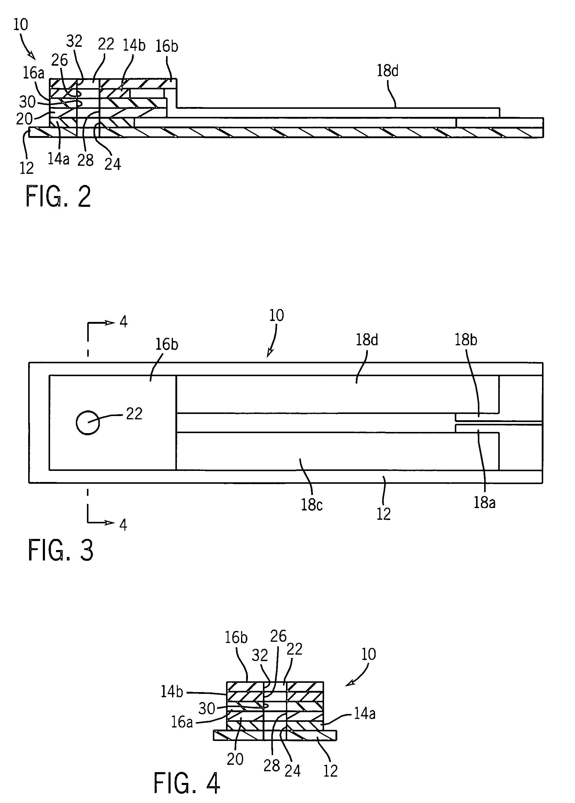
[0080]This example illustrates a multi-layer electrochemical cell for the determination of glucose. The conducting layers were formed on one major surface of an insulating substrate (polyvinyl chloride, approximately 450 micrometers thick). A conducting layer (carbon, approximately 15 μm thick) was deposited on a PVC substrate by means of screen-printing. The dimension of the individual cell after being trimmed was 5 mm wide and 40 mm long. However, in the actual case, a plurality of cells were prepared in one card and then cut into discrete cells having the dimensions described. The reagents, which consisted of glucose oxidase, ferrocene, and carbon (containing BES buffer, Clerol® antifoaming agent (Henkel-Nopco, Leeds, UK), and alginate binder), were screen-printed at a coating thickness of about 20 μm over a portion of the conducting layer of carbon. A Sericard® insulating layer (approximately 20 μm thick) was screen-printed over the entire area of the conducting layer, thereby l...
example 2
[0081]This example illustrates a multi-layer electrochemical cell for the determination of glucose. The conducting layers were formed on both major surfaces of an insulating substrate. A conducting layer comprising a mixture of carbon, glucose oxidase, and ferrocene was applied to a first major surface of a Melinex® insulating substrate by means of screen-printing so as to substantially cover the surface of the Melinex® insulating substrate, while leaving a portion on one of the ends of the first major surface of the Melinex® insulating substrate exposed to form an electrical contact area to allow removable connection to a measuring device. An insulating layer was then applied over the conducting layer by means of screen-printing in such a manner as to leave an area adjacent to the exposed portion of the insulating substrate exposed to form an electrical contact area to allow removable connection to a measuring device. A layer comprising a mixture of silver and silver chloride was t...
PUM
| Property | Measurement | Unit |
|---|---|---|
| volume | aaaaa | aaaaa |
| thickness | aaaaa | aaaaa |
| thickness | aaaaa | aaaaa |
Abstract
Description
Claims
Application Information


