Semiconductor chip, and semiconductor wafer including a variable thickness insulating layer

Active Publication Date: 2008-04-15
SAMSUNG ELECTRONICS CO LTD
View PDF32 Cites 48 Cited by
  • Summary
  • Abstract
  • Description
  • Claims
  • Application Information

AI Technical Summary

Benefits of technology

[0027]wherein the semiconductor substrate is formed so that the second surface rises higher in a region around the projection than in a region other than the region around the projection, and
[002

Problems solved by technology

In a conventional structure, a measure to prevent occurrence of sho

Method used


Image

  • Semiconductor chip, and semiconductor wafer including a variable thickness insulating layer
  • Semiconductor chip, and semiconductor wafer including a variable thickness insulating layer
  • Semiconductor chip, and semiconductor wafer including a variable thickness insulating layer

Examples


first embodiment

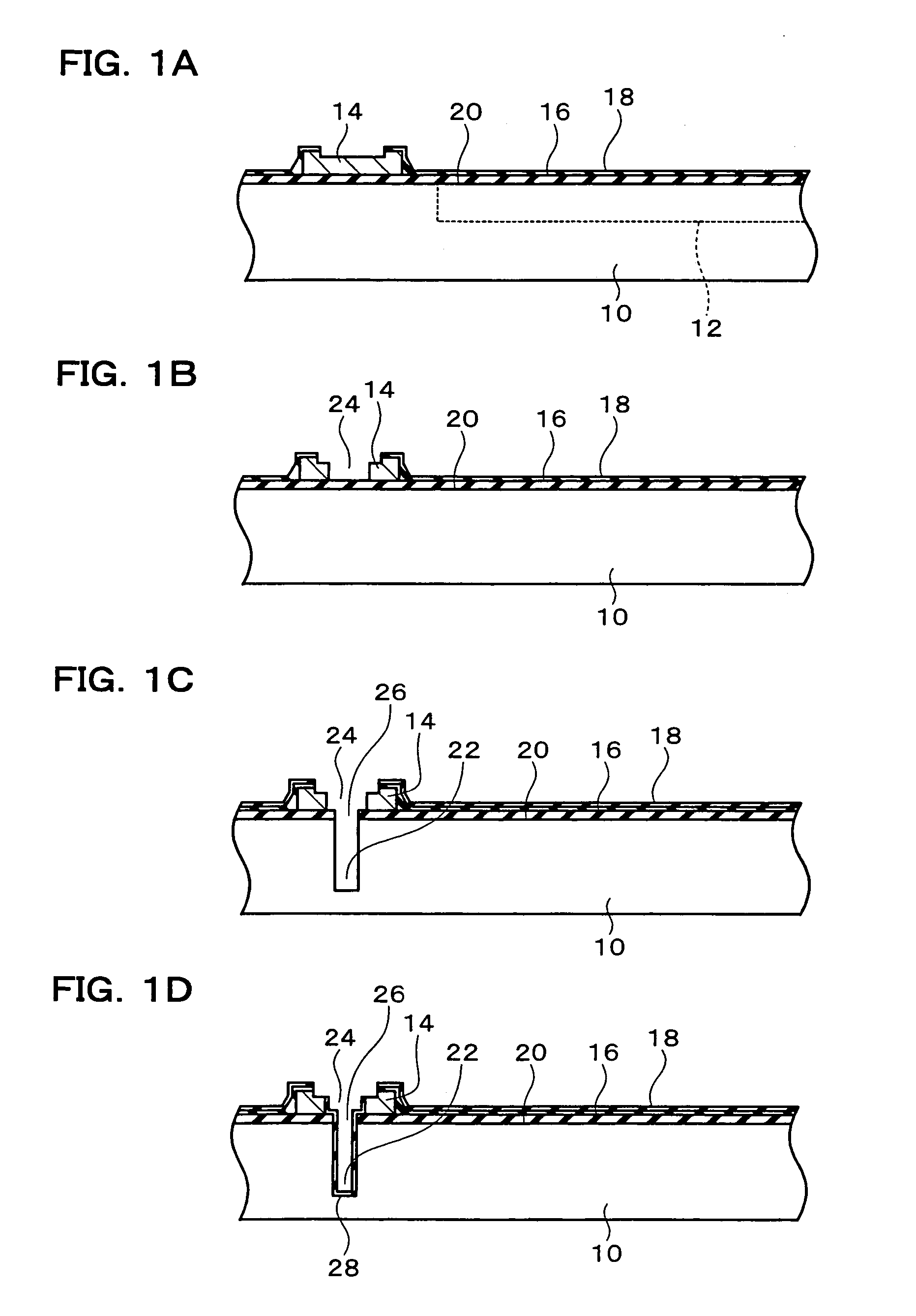
[0092](1) A semiconductor chip according to the present invention includes:

[0093]a semiconductor substrate;

[0094]an integrated circuit, at least a part of the integrated circuit being formed in the semiconductor substrate;

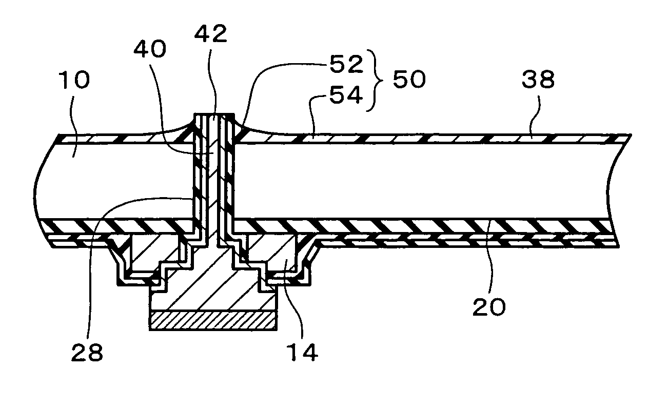
[0095]a penetrating electrode which is formed through the semiconductor substrate from a first surface to a second surface of the semiconductor substrate and has a projection which projects from the second surface; and

[0096]an insulating layer formed on the second surface except a part of the second surface, and in a region around the projection.

[0097]According to this semiconductor chip, since the insulating layer is formed in the region around the projection of the penetrating electrode except the region other than the region around the projection, occurrence of short circuits can be prevented by sufficiently securing the gap between stacked semiconductor chips. Moreover, filling capability of an underfill can be improved by sufficiently securing the gap between ...

second embodiment

[0099](3) A semiconductor chip according to the present invention includes:

[0100]a semiconductor substrate;

[0101]an integrated circuit, at least a part of the integrated circuit being formed in the semiconductor substrate;

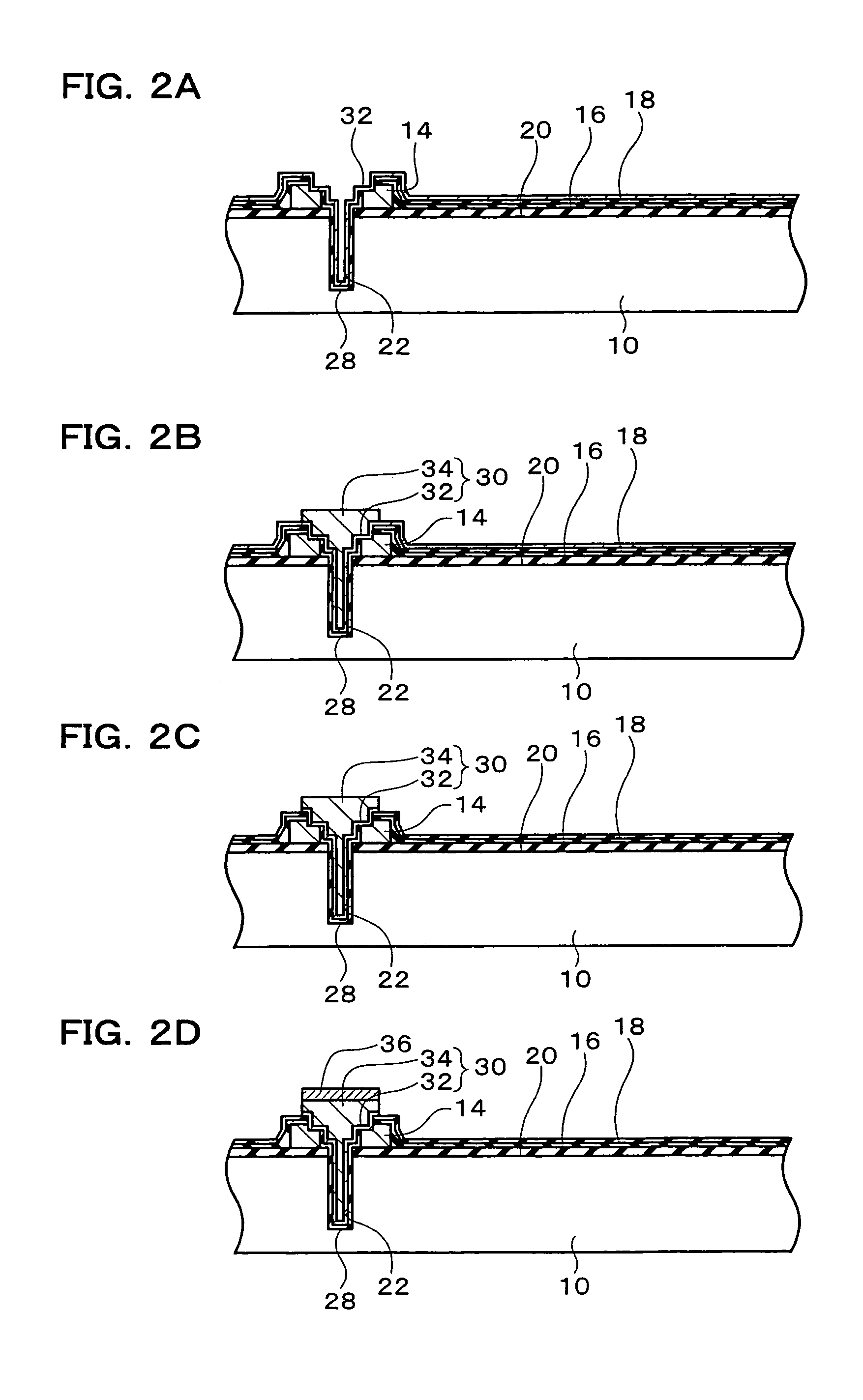
[0102]a penetrating electrode which is formed through the semiconductor substrate from a first surface to a second surface of the semiconductor substrate and has a projection which projects from the second surface;

[0103]an insulating layer formed over an entire surface of the second surface,

[0104]wherein the insulating layer includes a first insulating section formed in a region around the projection and a second insulating section other than the first insulating section, and

[0105]wherein the second insulating section is formed to be thinner than a thickest area of the first insulating section.

[0106]According to this semiconductor chip, since the second insulating section is formed to be thinner than the thickest area of the first insulating section, occurrence of ...

third embodiment

[0108](5) A semiconductor chip according to the present invention includes:

[0109]a semiconductor substrate;

[0110]an integrated circuit, at least a part of the integrated circuit being formed in the semiconductor substrate;

[0111]a penetrating electrode which is formed through the semiconductor substrate from a first surface to a second surface of the semiconductor substrate and has a projection which projects from the second surface;

[0112]an insulating layer formed on the second surface except a part of the second surface, and in a region around the projection,

[0113]wherein the semiconductor substrate is formed so that the second surface rises higher in the region around the projection than in a region other than the region around the projection.

[0114]According to this semiconductor chip, since the second surface is formed to rise higher in the region around the projection than in the region other than the region around the projection, occurrence of short circuits can be prevented by...


PUM


Abstract

A semiconductor chip includes: a semiconductor substrate; a penetrating electrode which is formed through the semiconductor substrate from a first surface to a second surface of the semiconductor substrate and has a projection which projects from the second surface; an insulating layer formed over an entire surface of the second surface. The insulating layer includes a first insulating section formed in a region around the projection and a second insulating section other than the first insulating section. The second insulating section is formed to be thinner than a thickest area of the first insulating section.

Description

CROSS-REFERENCE TO RELATED APPLICATIONS[0001]This application claims the benefit of Japanese patent application 2003-007281, filed Jan. 15, 2003. The disclosure of the above application is incorporated herein by reference in its entirety.BACKGROUND OF THE INVENTION[0002]The present invention relates to a semiconductor chip, a semiconductor wafer, a semiconductor device and a method of manufacturing the same, a circuit board, and an electronic instrument.[0003]A semiconductor device in three-dimensional mounting form has been developed. It is known in the art that penetrating electrodes are formed in semiconductor chips, and the semiconductor chips are stacked to bond the penetrating electrodes. In a conventional structure, a measure to prevent occurrence of short circuits between the stacked semiconductor chips is insufficient. An insulating layer may be formed on the surface of the semiconductor chip on which the penetrating electrodes are formed. In this case, the gap for filling ...

Claims


Application Information

Patent Timeline
IPC IPC(8): H01L29/40H01L23/48H01L23/485H01L25/065H01L29/41H01L21/3205H01L21/52H01L23/12H01L23/52H01L25/07H01L25/18H05K3/30
CPCH01L23/481H01L24/02H01L25/0657H01L2924/07802H01L2224/0401H01L2225/06513H01L2225/06541H01L2924/01004H01L2924/01005H01L2924/01006H01L2924/01011H01L2924/01013H01L2924/01014H01L2924/01022H01L2924/01027H01L2924/01029H01L2924/01033H01L2924/0105H01L2924/01074H01L2924/01078H01L2924/014H01L2924/14H01L2924/15311H01L2924/19043H01L2224/13009H01L2224/16146H01L2924/00H01L2924/12042H01L2224/02372H01L2224/05548H01L24/05H01L24/13H01L24/16H04M1/035
Inventor HARA, KAZUMI
Owner SAMSUNG ELECTRONICS CO LTD
Why Eureka
Try Eureka