Wafer bonded pressure sensor

a pressure sensor and wafer technology, applied in the field of pressure sensors, can solve the problems of sensor calibration drift, sensor damage, reference cavity pressure equilibration with tire pressure, etc., and achieve the effects of low melting point material, high voltage, and avoiding high surface cleanliness

Inactive Publication Date: 2006-04-20
PRECISION MECHATRONICS
View PDF14 Cites 42 Cited by
  • Summary
  • Abstract
  • Description
  • Claims
  • Application Information

AI Technical Summary

Benefits of technology

[0097] Optionally, the wafer bonding is direct wafer bonding wherein the contacting surfaces of the first and second wafers are ultra clean, and activated by making them hydrophilic or hydrophobic prior to bonding, and then brought into contact at high temperature, preferably around 1000° C. Anodic bonding offers another option wherein the contacting surfaces of the first and second wafers have a large voltage applied across them. The wafers may be in a vacuum, air or an inert gas when the bond is formed. Intermediate layer bonding is a third option wherein a layer of low melting point material is applied to one or both of the contacting surfaces of the first and second wafers so that heat and pressure forms the wafer bond. Preferably the low melting point material is silicon nitride or titanium nitride. This option avoids the high surface cleanliness required by direct silicon bonding and the high voltages required by anodic bonding.

Problems solved by technology

sensors for other steam based machines where overpressure can lead to destruction and loss of life
The impetus for this development comes from recent Firestone / Ford Explorer incidents which led to a number of fatal accidents.
If the reference fluid leaks, the sensor suffers calibration drift.
The permeability of the seal closing the backside of the wafer is the main cause of leakage.
However, the air permeability of polymeric adhesive would result in the reference cavity pressure equilibrating with the tire pressure in about 100 days.
This is clearly unsuitable.
The calibration drift would be unacceptable within a year.

Method used


Image

  • Wafer bonded pressure sensor
  • Wafer bonded pressure sensor
  • Wafer bonded pressure sensor

Examples


Embodiment Construction

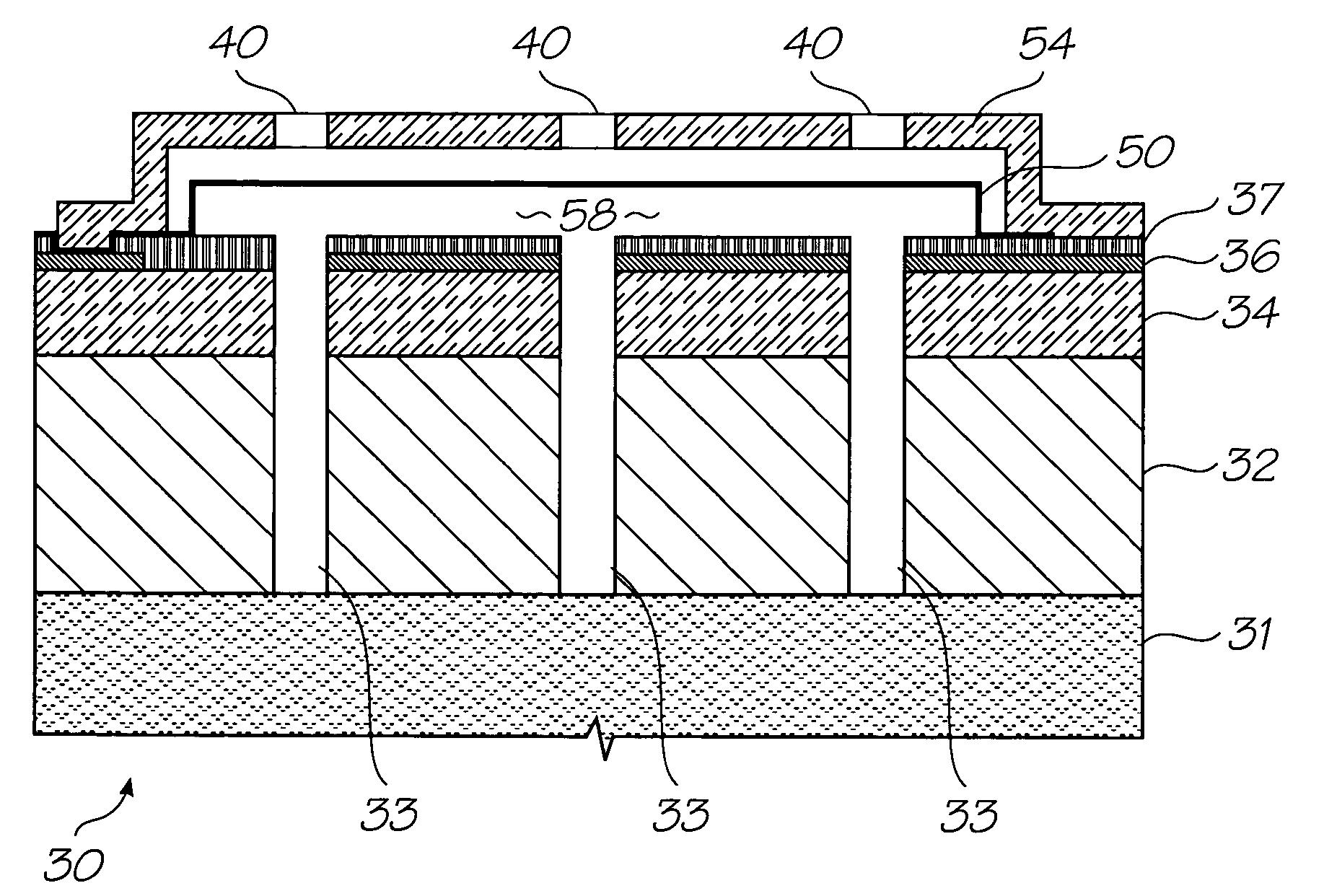
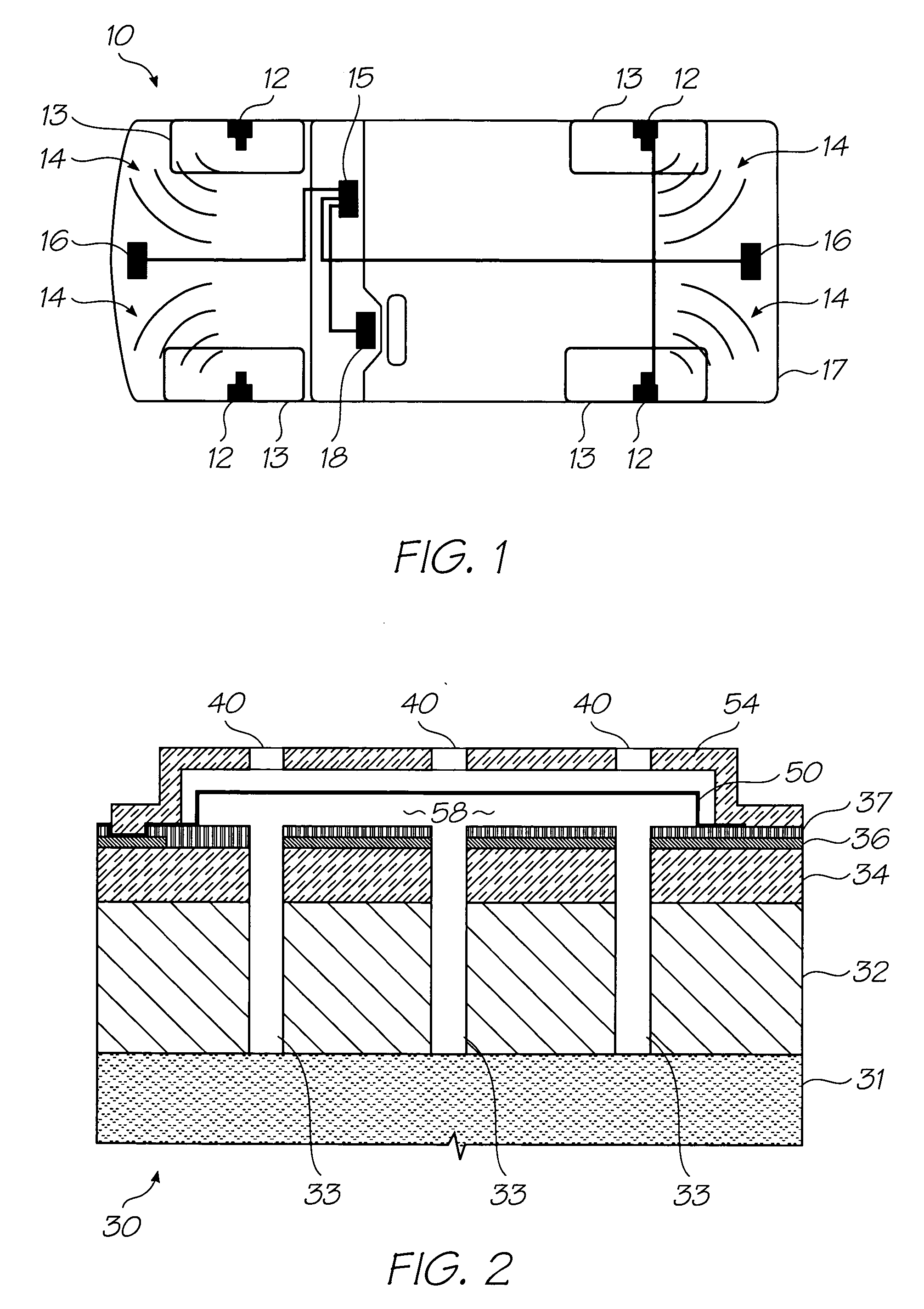
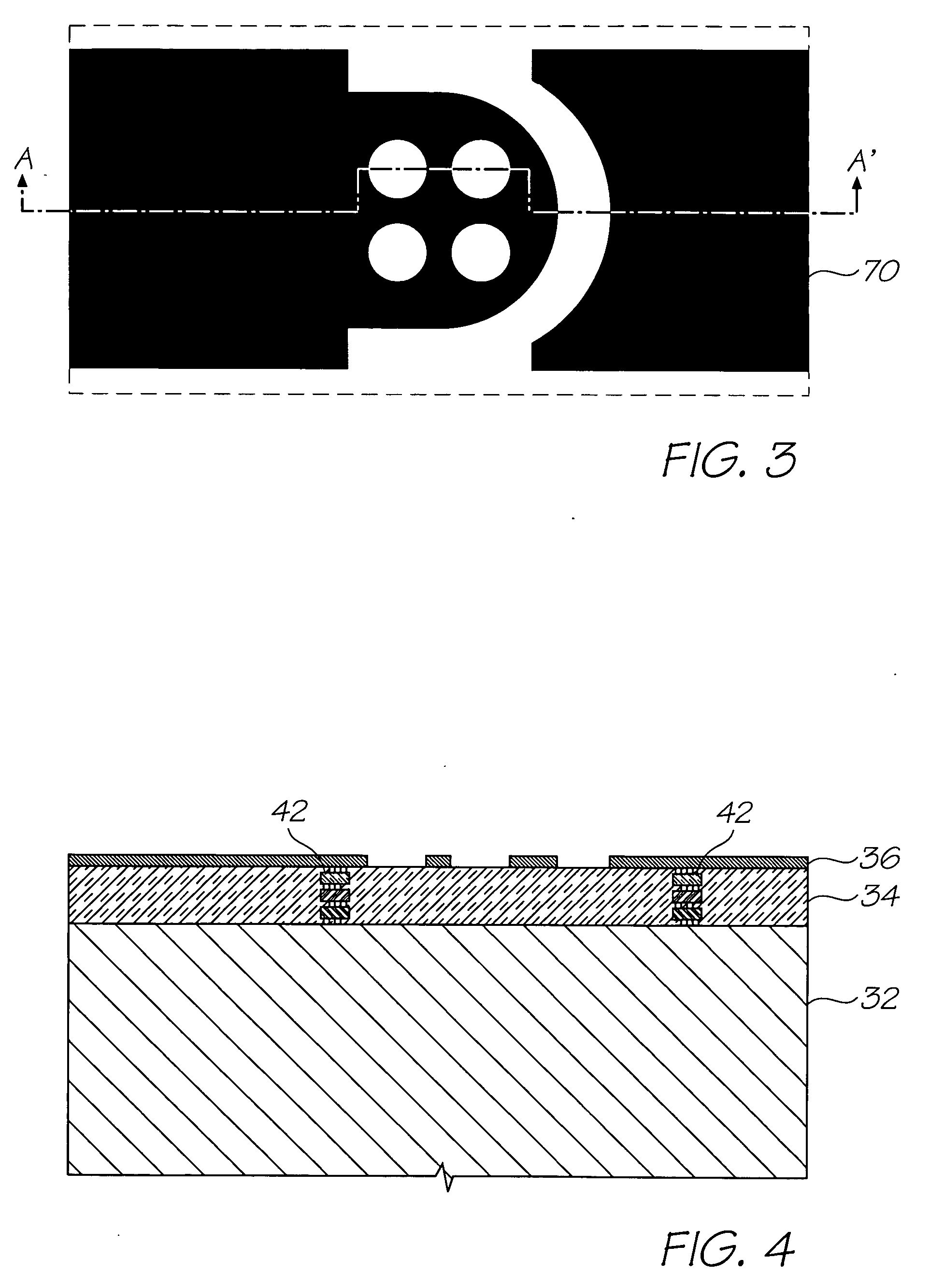
[0113] The following embodiments are described in order to provide a more precise understanding of the subject matter of the present invention. While the embodiments focus on a capacitative type sensor, ordinary workers in this field will readily understand that the invention is equally applicable to other forms of pressure sensor such as: [0114] (i) Piezo-resistive, where the membrane is formed from a non-conductive material and the piezo material is in contact with the membrane. Deflections of the membrane give rise to piezo-induced changes in resistivity (and hence current, if a voltage is applied) that can be monitored electronically. [0115] (ii) Resonant pressure sensors, where the frequency of oscillation of the membrane depends on the pressure difference. The initial resonance could be activated by using a time-varying electrostatic force between the two electrodes. [0116] (iii) Force compensation pressure sensors, where an electrostatic force is applied to maintain the membr...


PUM

PropertyMeasurementUnit
temperatureaaaaaaaaaa
thickaaaaaaaaaa
diameteraaaaaaaaaa

Abstract

A pressure sensor (30) for sensing a fluid pressure in harsh environments such as the air pressure in a tire, by using a first wafer substrate (32) with a front side and an opposing back side, a chamber (58) partially defined by a flexible membrane (50) formed on the front side and at least one hole (33) etched from the back side to the chamber (58);
    • a second wafer (31) on the back side of the first wafer (32) to seal the at least one hole (33); wherein,
    • the chamber (58) containing a fluid at a reference pressure, such that the flexible membrane (50) deflects due to pressure differentials between the reference pressure and the fluid pressure; and,
    • associated circuitry (34) for converting the deflection of the flexible membrane (50) into an output signal indicative of the fluid pressure; wherein,
    • the second wafer (31) is wafer bonded to the first wafer substrate (32). Wafer bonding offers an effective non-adhesive solution. It provides a hermetic seal with only minor changes to the fabrication procedure. Skilled workers in this field will readily understand that the most prevalent forms of wafer bonding are: direct wafer, or silicon fusion, bonding; anodic, or electrostatic Mallory process bonding; and, intermediate layer bonding.

Description

TECHNICAL FIELD The present invention generally relates to a pressure sensor and in particular, a micro-electro mechanical (MEMS) pressure sensor. CO-PENDING APPLICATIONS [0001] Various methods, systems and apparatus relating to the present invention are disclosed in the following co-pending applications filed by the applicant or assignee of the present invention simultaneously with the present application: TPS001USTPS002USTPS003USTPS004USTPS006USTPS007USTPS008USTPS009USTPS010USTPS011USTPS012US The disclosures of these co-pending applications are incorporated herein by cross-reference. Each application is temporarily identified by its docket number. This will be replaced by the corresponding USSN when available. CROSS REFERENCES TO RELATED APPLICATIONS [0002] The following patents or patent applications filed by the applicant or assignee of the present invention are hereby incorporated by cross-reference. 09 / 113,07810 / 868,86610 / 043,30010 / 043,29910 / 129,50210 / 043,35010 / 129,50110 / 04...

Claims


Application Information

Patent Timeline
Patent Type & Authority Applications(United States)
IPC IPC(8): G01L9/00
CPCB60C23/0408
Inventor SILVERBROOK, KIAMALLINSON, SAMUEL GEORGE
Owner PRECISION MECHATRONICS
Why Eureka
Try Eureka