Liquid crystal display panel and thin film transistor array

a thin film transistor and display panel technology, applied in non-linear optics, instruments, optics, etc., can solve the problems of affecting the performance of pixels of the display panel, damage to the reliability of the thin film transistor, and charge leakage, so as to improve the capacitance of capacitors, reduce the area of common lines, and improve the performance of the liquid crystal display panel

Active Publication Date: 2008-04-22
AU OPTRONICS CORP
View PDF3 Cites 9 Cited by
  • Summary
  • Abstract
  • Description
  • Claims
  • Application Information

AI Technical Summary

Benefits of technology

[0011]Accordingly, the present invention is directed to a thin film transistor array for preventing charge leakage of capacitors due to the pollution of particles and for enhancing the capacitance of capacitors to improve the performance of liquid crystal display panels, without altering the aperture ratio and reliability of transistors.
[0021]In the present invention, the branches of the common lines are used to increase the capacitance of the capacitors such that the performance of the liquid crystal display panels can be improved. Therefore, even if the area of the common lines is reduced, the capacitance lost due to the reduced area of the common lines can be compensated by the capacitance of capacitors comprising the branches and the pixel electrodes. Therefore, in the present invention, capacitance leakage between the common lines and the pixel electrodes can be prevented.

Problems solved by technology

However, a thinned-out gate insulator 210 and / or protection layer 220 may damage the reliability of the thin film transistors.
In addition, particles may fall in the gate insulator and / or the protection layer or cracks may be formed therein due to flaws during the manufacturing process, which will ultimately lead to charge leakage.
As a result, the performance of pixels of the display panel is impaired and the display quality is brought down.

Method used


Image

  • Liquid crystal display panel and thin film transistor array
  • Liquid crystal display panel and thin film transistor array
  • Liquid crystal display panel and thin film transistor array

Examples


Embodiment Construction

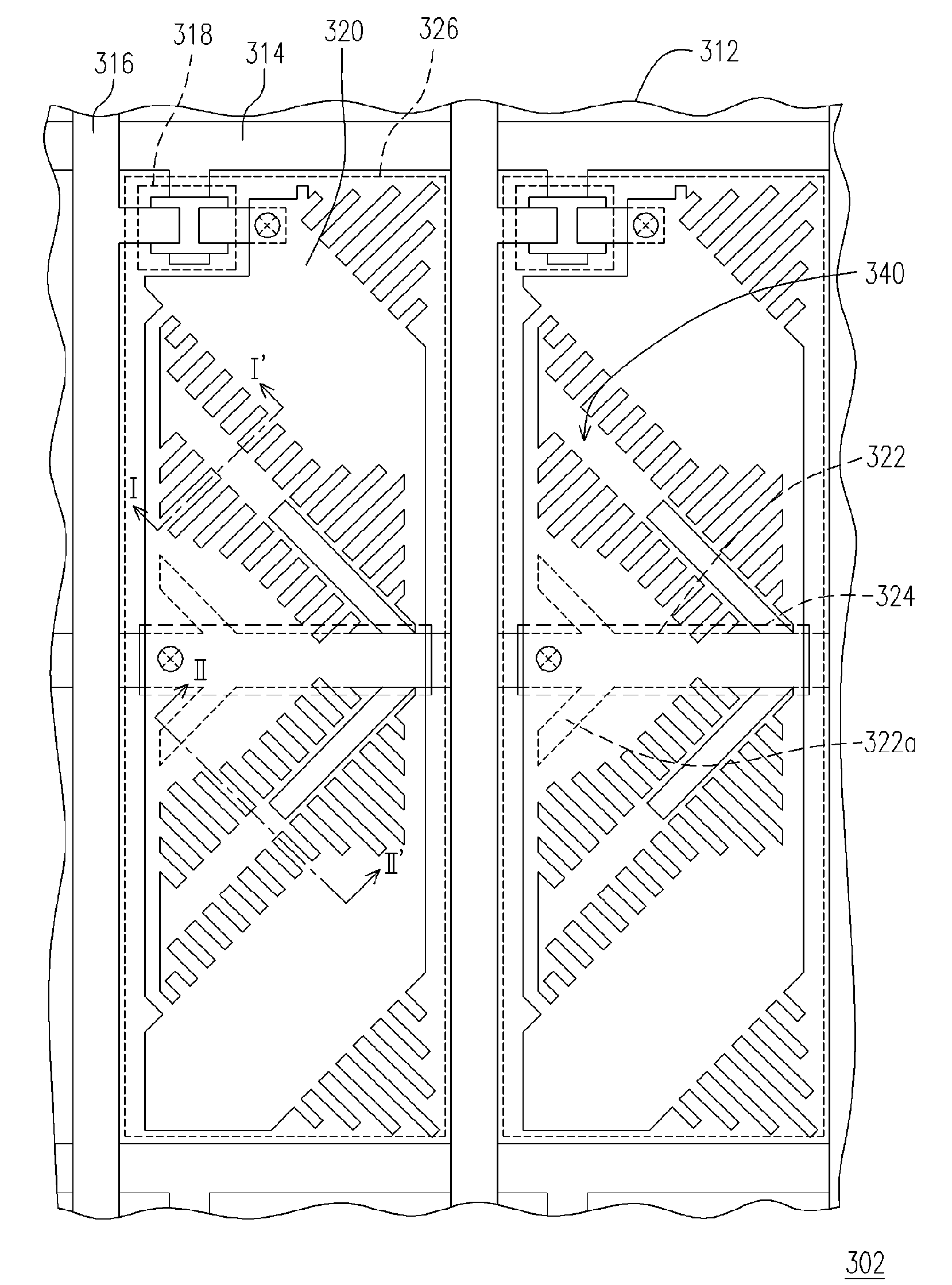
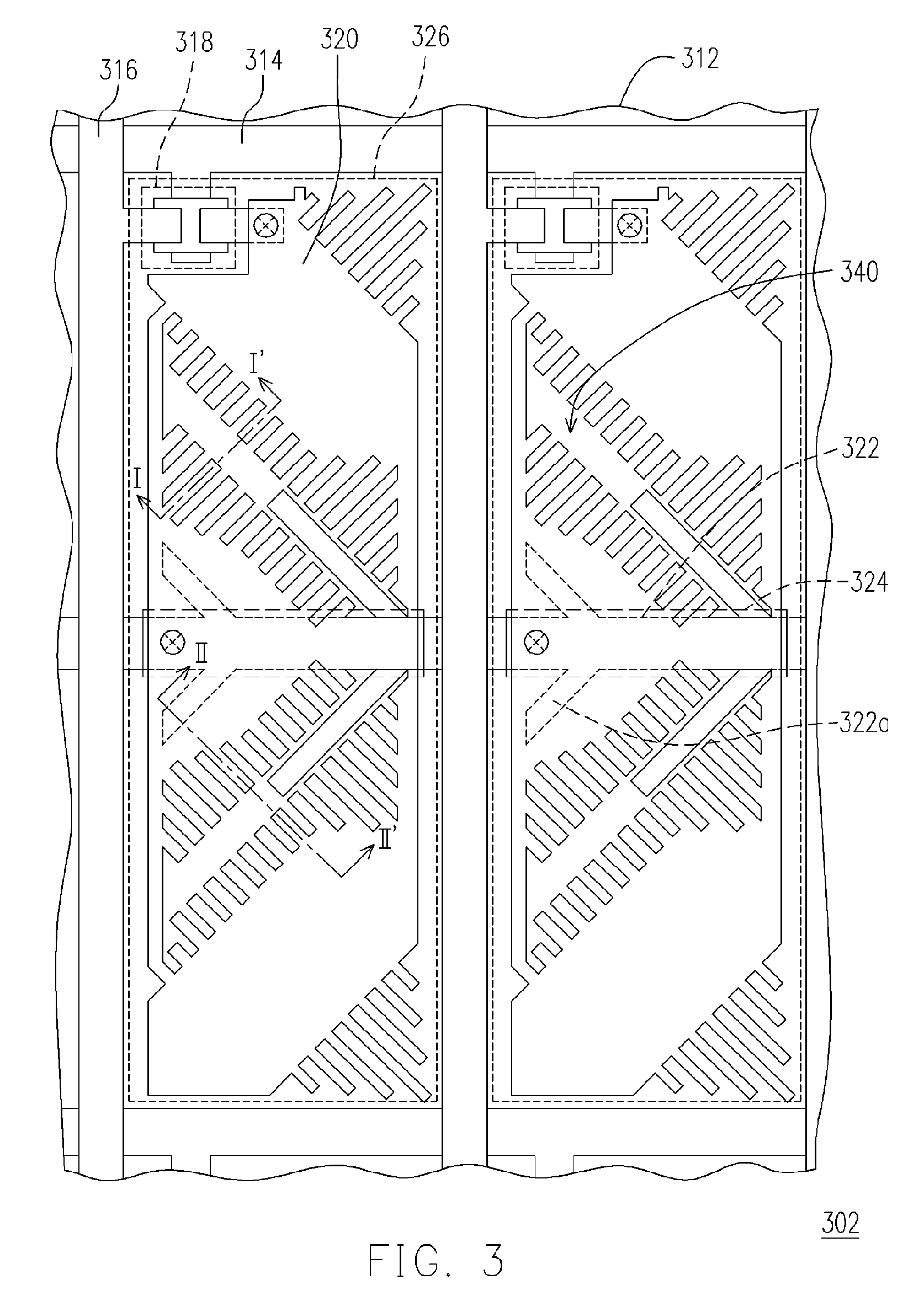
[0034]In the present invention, the common lines with the branches are used to enhance capacitance. Wherein, these branches of the common lines are disposed in corresponding positions to pixels where the luminance quality is bad to reduce the impact on the aperture ratio. What follows are descriptions of some embodiments in the present invention.

[0035]FIG. 3 is a schematic top view showing a partial thin film transistor array according to an embodiment of the present invention. FIG. 4 is a schematic configuration showing a decomposed Multi-Domain Vertical Alignment (MVA) liquid crystal display panel comprising the thin film transistor array in FIG. 3 according to an embodiment of the present invention. As shown in FIG. 4, the thin film transistor array 302, the color filter 304 and the liquid crystal layer 306 constitute the MVA liquid crystal display panel 300. Wherein, the liquid crystal layer 306 comprises a plurality of liquid crystal molecules (not shown). The color filter 304 ...


PUM

PropertyMeasurementUnit
storage capacitanceaaaaaaaaaa
voltagesaaaaaaaaaa
areaaaaaaaaaaa

Abstract

A thin film transistor array comprising a plurality of common lines for providing the storage capacitance of pixels is provided. In particular, each of the common lines comprises a plurality of branches. Wherein, the common line and the branches thereof, and the pixel electrode constitute the storage capacitor. The branches are disposed at pixels where the luminance quality is bad. Therefore, the storage capacitance of the pixels can be enhanced without altering the aperture ratio of the pixels. Accordingly, the performance of the liquid crystal display panel can be improved.

Description

CROSS-REFERENCE TO RELATED APPLICATION[0001]This application claims the priority benefit of Taiwan application serial no. 93122690, filed Jul. 29, 2004.BACKGROUND OF THE INVENTION[0002]1. Field of the Invention[0003]The present invention relates to a display apparatus, and more particularly, to a liquid crystal display panel, a thin film transistor array capable of enhancing storage capacitance thereof and a capacitor structure.[0004]2. Description of the Related Art[0005]The rapid development of semiconductor and display technologies has opened the door to a multi-media society. Among display apparatus, thin film transistor liquid crystal displays (TFT-LCDs) have such advantages as high image quality, excellent space-efficiency, low power consumption and non-radiation and have gradually dominated the display market.[0006]A TFT-LCD mainly comprises a thin film transistor array, a color filter and a liquid crystal layer. Wherein, the thin film transistor array comprises a plurality o...

Claims


Application Information

Patent Timeline
Patent Type & Authority Patents(United States)
IPC IPC(8): G02F1/1368G02F1/1337G02F1/139G02F1/1343
CPCG02F1/133707G02F1/133753G02F1/136213G02F1/1393
Inventor LAI, HAN-CHUNG
Owner AU OPTRONICS CORP
Why Eureka
Try Eureka