

Method and apparatus for arranging recipe of scanning electron microscope and apparatus for evaluating shape of semiconductor device pattern
a scanning electron microscope and semiconductor device technology, applied in material analysis using wave/particle radiation, instruments, nuclear engineering, etc., can solve the problem of not being able to select appropriate imaging points, and achieve the effect of rapid adaptation to process changes and easy establishmen
- Summary
- Abstract
- Description
- Claims
- Application Information
AI Technical Summary
Benefits of technology
Problems solved by technology
Method used
Image

Examples
Embodiment Construction
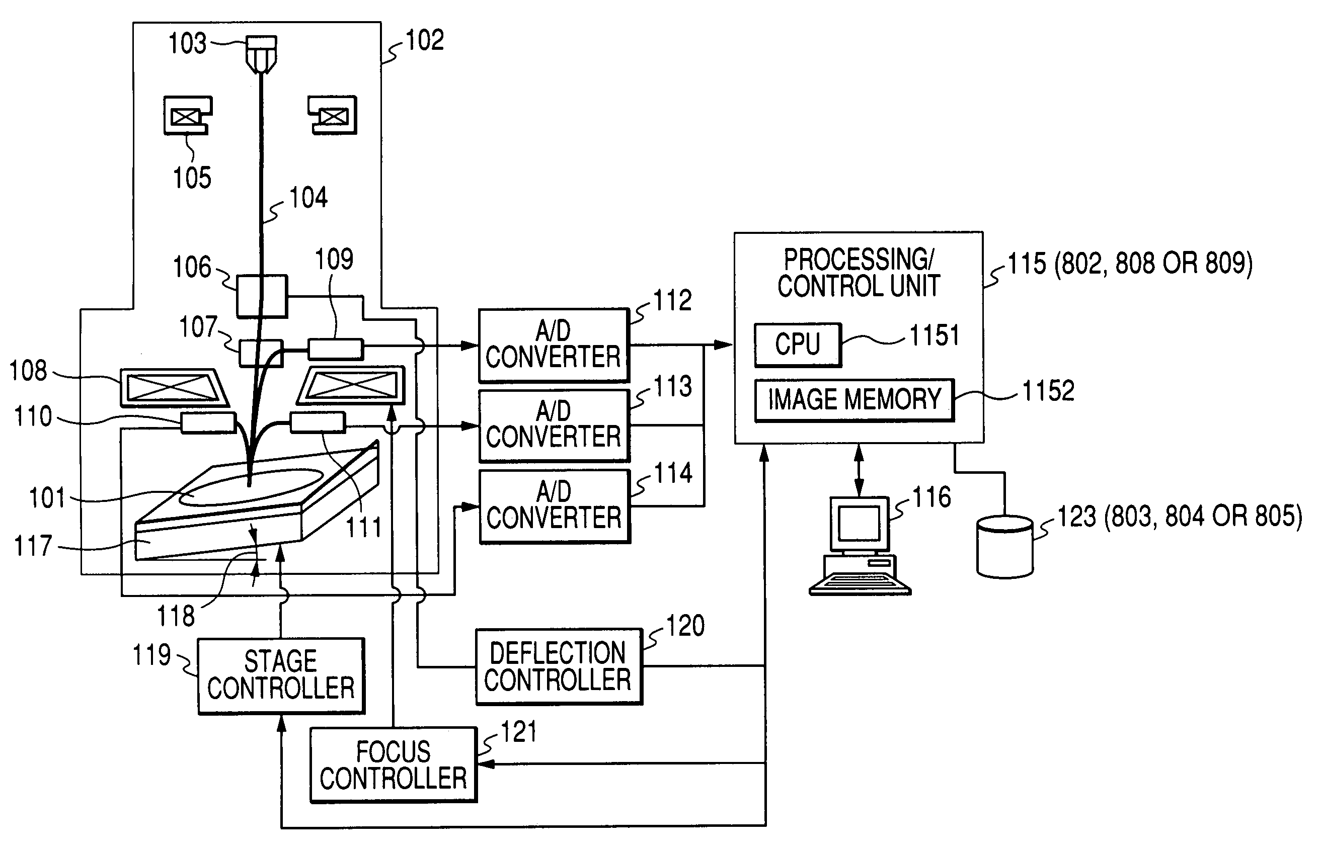
[0039]Embodiments of a SEM apparatus with an imaging recipe arrangement function according to the present invention, namely, a semiconductor pattern shape evaluation apparatus using a scanning electron microscope such as a critical-dimension scanning electron microscope (CD-SEM), will be described hereunder using FIGS. 1 to 12.
[0040]The number of inspection portions that require dimensional management of semiconductor patterns may be increasing greatly because of factors for such as decreases in design margins according to making minutely and making high density of LSI patterns. These tendencies are bringing about a strong demand for the improvement of the throughput and automation ratio of a SEM apparatus or like apparatus used as a dimensional management tool.
[0041]To use a SEM apparatus (or the like) for performing SEM-based observations for the critical points as dimension-measuring points on the semiconductor pattern to be inspected, and evaluating pattern shapes by measuring t...
PUM
 Abstract
Description
Claims
Application Information