
Sensing circuit for multi-level flash memory

a sensing circuit and flash memory technology, applied in the field of sensing circuits for multi-level flash memory, can solve the problems of limited storage capacity becoming a disadvantage, limited storage capacity being provided to generate the required number of reference voltage levels, and the limitation of one memory cell being able to distinguish only two different states, etc., to achieve the effect of reducing the global circuit dimension and reducing the testing time for reference voltage calibration

Inactive Publication Date: 2008-05-06
WINBOND ELECTRONICS CORP
View PDF4 Cites 13 Cited by
  • Summary
  • Abstract
  • Description
  • Claims
  • Application Information

AI Technical Summary

Benefits of technology

The solution reduces circuit dimension and calibration time, enabling efficient data storage with stable reference voltages, enhancing storage capacity and production efficiency.

Problems solved by technology

However, such conventional memory has the limitation that one memory cell can distinguish only two different states, i.e., one memory cell can store only one-bit of data.
As a result, limited storage capacity becomes a disadvantage of conventional memory device.
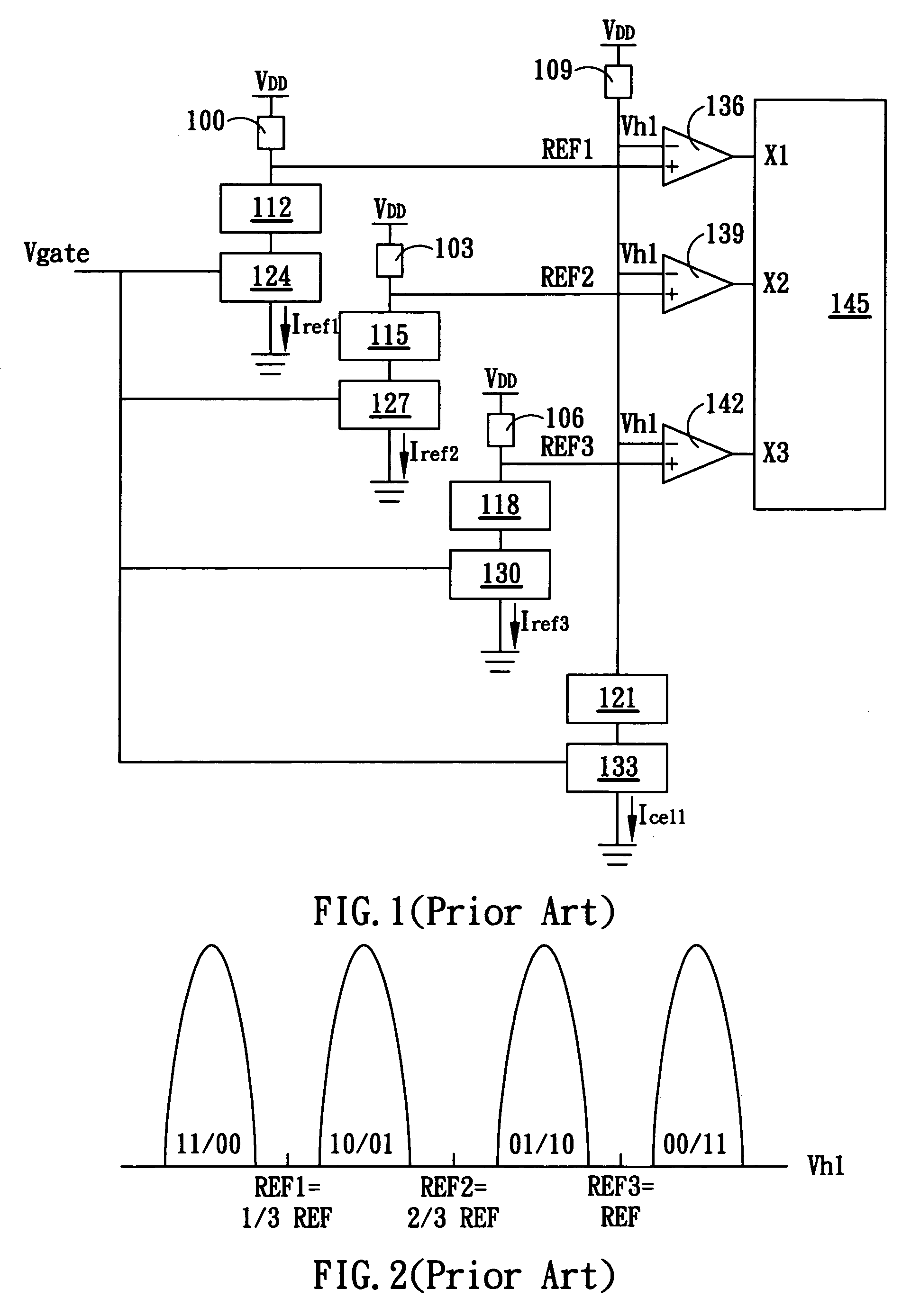
A disadvantage of the circuit shown in FIG. 1 is, however, that the same number of reference voltage generating units must be provided to generate the required number of reference voltage levels.

Method used


Image

  • Sensing circuit for multi-level flash memory
  • Sensing circuit for multi-level flash memory
  • Sensing circuit for multi-level flash memory

Examples


Embodiment Construction

[0018]The detailed description of the present invention will be discussed in the following embodiment, which is not intended to limit the scope of the present invention, but can be adapted for other applications.

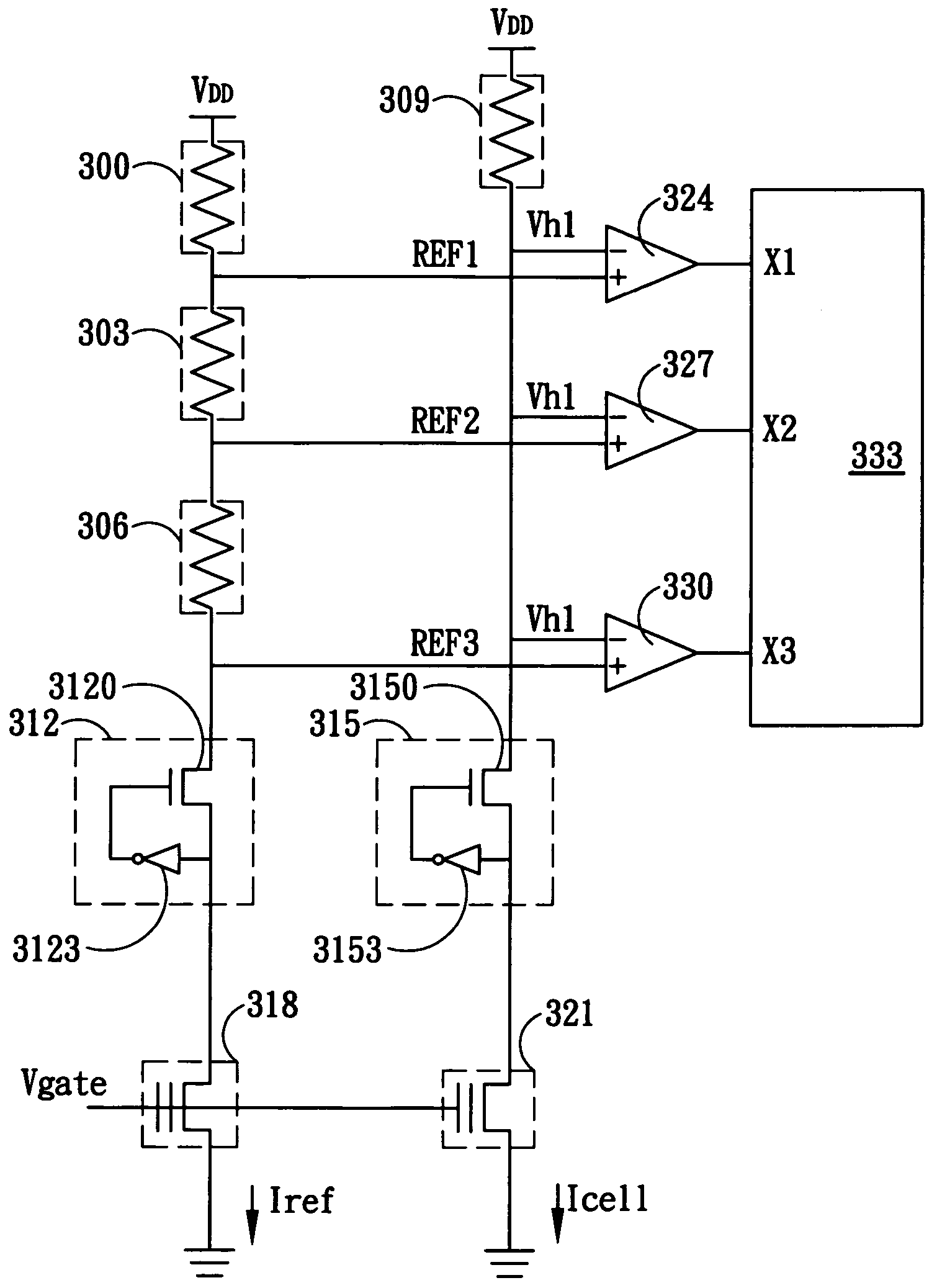
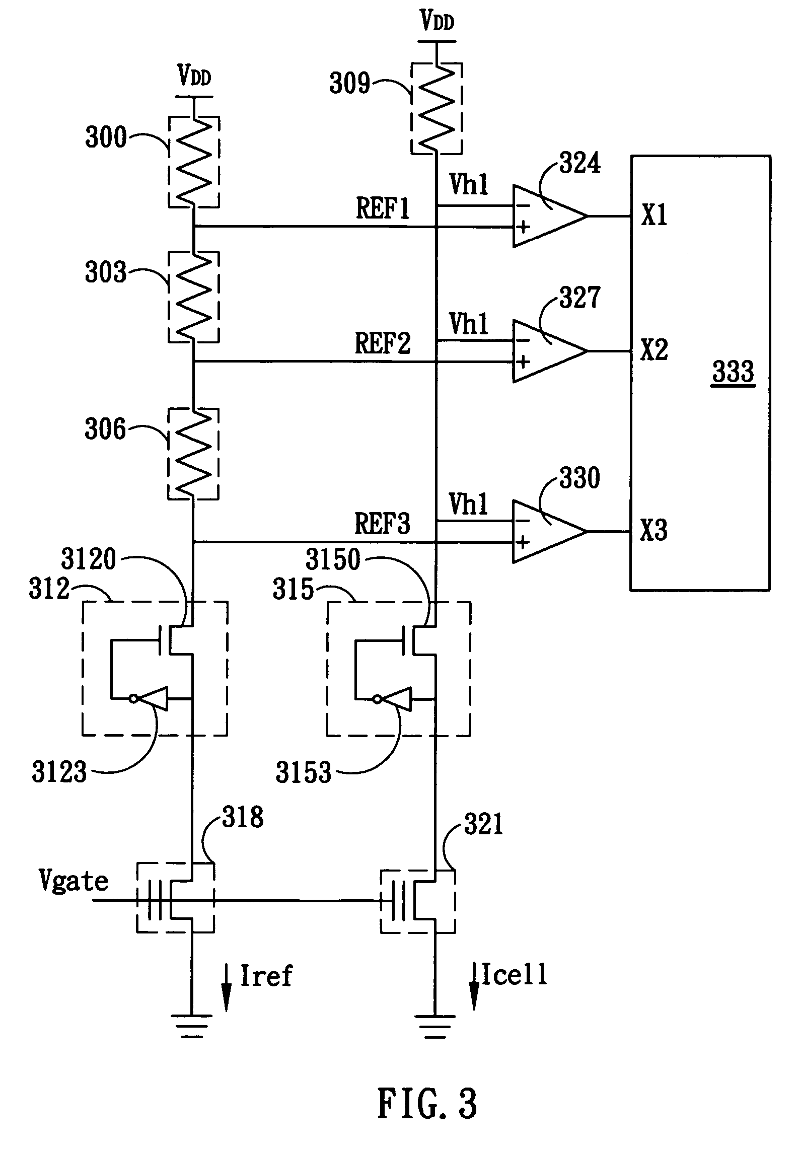
[0019]The present invention discloses a sensing circuit for multi-level flash memory capable of reducing global circuit dimension as well as decreasing the reference voltage calibration time. FIG. 3 shows the circuit diagram of one embodiment according to present invention. The diagram includes a reference voltage generator, a data saving circuit, a comparing circuit, and a decoder 333. The reference voltage generator contains a first resistive device 300, a second resistive device 303, a third resistive device 306, a first bit line clamp circuit 312, and a reference memory cell 318. Terminals of the first resistive device 300 are respectively connected to a voltage source VDD and the first terminal of the second resistive device 303. The second terminal of the second resist...


PUM


Abstract

A sensing circuit for multi-level flash memory is disclosed. The advantages of the sensing circuit are reducing the circuit size, reducing the testing time for tuning reference voltage and maintaining a constant difference between two approximate reference voltages. The sensing circuit comprises a reference voltage generator which includes a number of serial connected resistive devices and provides several reference voltages by voltage division; a data saving circuit outputs a data voltage; a comparing circuit compares the data voltage with the several reference voltages to output a comparing signal; a decoder receives and then decodes the comparing signal to output the data.

Description

BACKGROUND OF THE INVENTION[0001]1. Field of the Invention[0002]The present invention generally relates to a sensing circuit for multi-level flash memory, and more particularly to a sensing circuit for multi-level flash memory by using voltage division to provide reference voltages.[0003]2. Description of the Prior Art[0004]In conventional memory devices, data is stored in a flash memory cell in the form of electrical charge accumulated inside an inner gate, which is known as a floating gate. The amount of charge stored in the floating gate depends on the voltage applied to the external gate of the memory cell that controls the magnitude of electrical current flowing through it. The data state “0”, or “1”represented by the memory cell depends on whether threshold voltage generated by the stored charge exceeds a specified threshold voltage or not. However, such conventional memory has the limitation that one memory cell can distinguish only two different states, i.e., one memory cell...

Claims


Application Information

Patent Timeline
Patent Type & Authority Patents(United States)
IPC IPC(8): G11C11/34G11C16/06
CPCG11C11/5642G11C16/28
Inventor HUANG, CHUNG-MENG
Owner WINBOND ELECTRONICS CORP
Learn More