Semiconductor layout structure and testing method thereof

a technology of semiconductors and layouts, applied in semiconductor/solid-state device testing/measurement, measurement devices, instruments, etc., can solve the problems of small testing area and less testing time, and achieve the effect of reducing error bars, easy increasing the number of mos transistors, and less testing tim

Inactive Publication Date: 2014-12-04
UNITED MICROELECTRONICS CORP
View PDF12 Cites 9 Cited by
  • Summary
  • Abstract
  • Description
  • Claims
  • Application Information

AI Technical Summary

Benefits of technology

[0006]The invention is directed to a semiconductor layout structure and a testing method thereof. A plurality of metal-oxide-semiconductor (MOS) transistors are arranged for testing. The semiconductor layout structure and the testing method thereof do not need any extra wafer acceptance test (WAT) tool. Further, the number of the MOS transistors can be easily increased to reduce the error bar due to the high sample size. Moreover, even if the number of the MOS transistors is large, the testing time is still less and the testing area is still small.

Problems solved by technology

Moreover, even if the number of the MOS transistors is large, the testing time is still less and the testing area is still small.

Method used


Image

  • Semiconductor layout structure and testing method thereof
  • Semiconductor layout structure and testing method thereof
  • Semiconductor layout structure and testing method thereof

Examples


Embodiment Construction

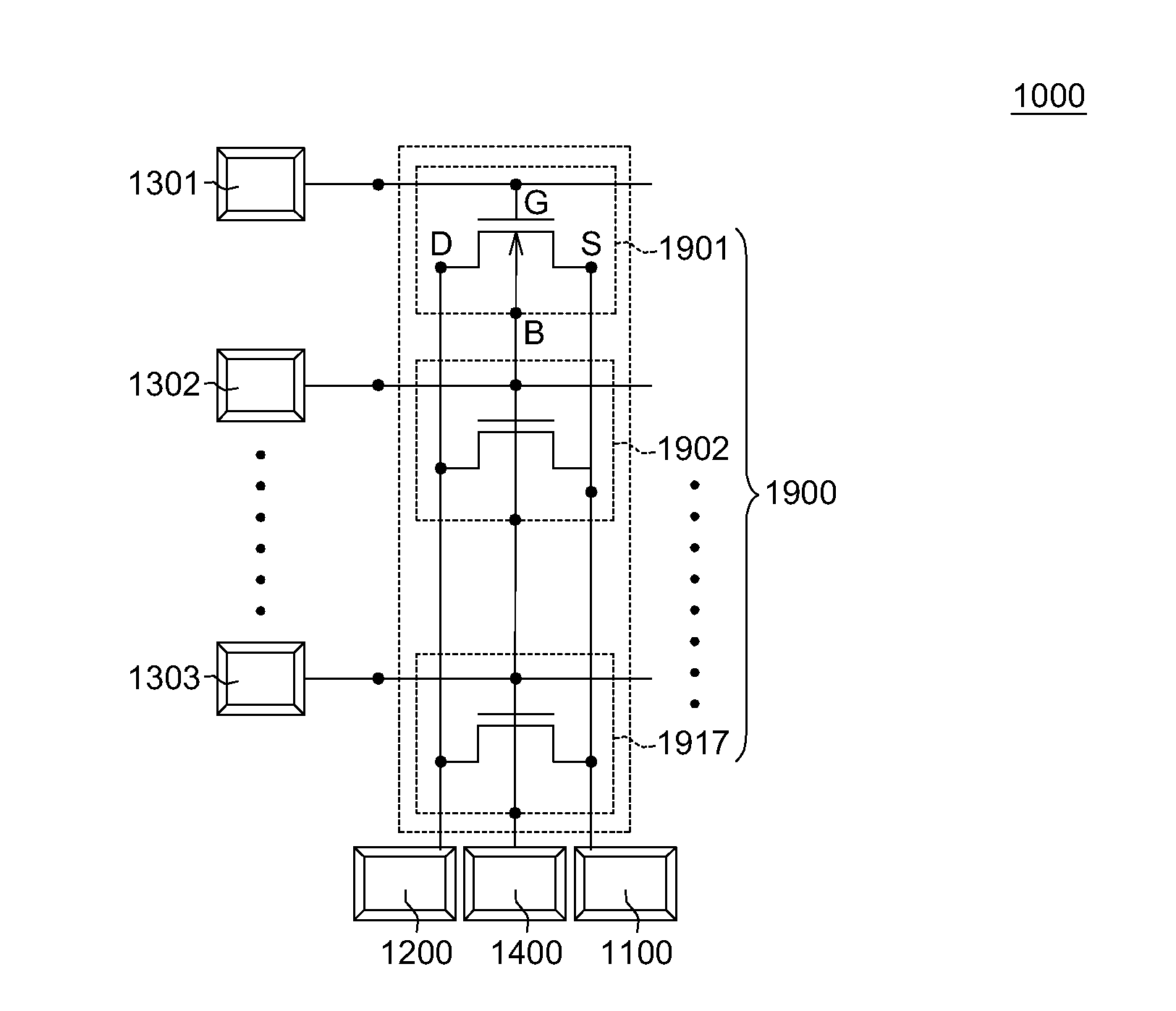
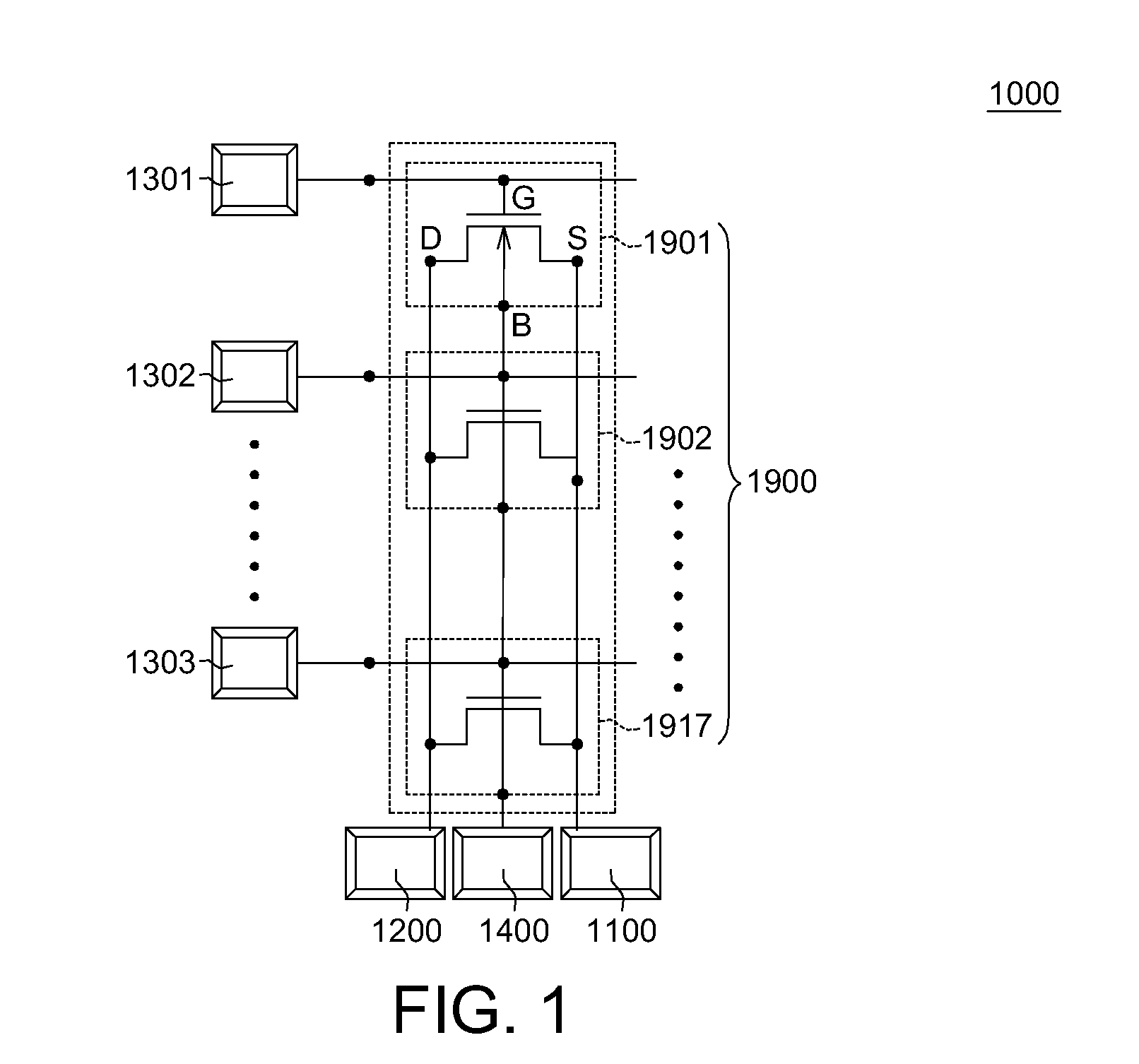
[0015]Please referring to FIG. 1, FIG. 1 illustrates a circuit diagram of a semiconductor layout structure 1000 according to one embodiment of the invention. The semiconductor layout structure 1000 includes a device under test (DUT) 1900, a first testing pad 1100, a second pad 1200, a plurality of third testing pads 1301, 1302, . . . , 1317 and a fourth testing pad 1400. The DUT 1900 is a semiconductor device, such as multiple MOSFET, memory cell, interconnect routing structure, passive device. The first testing pad 1100, the second test pad 1200, the third testing pads 1301, 1302, . . . , 1317 and the fourth testing pad 1400 are used for being applied voltages during a testing process.

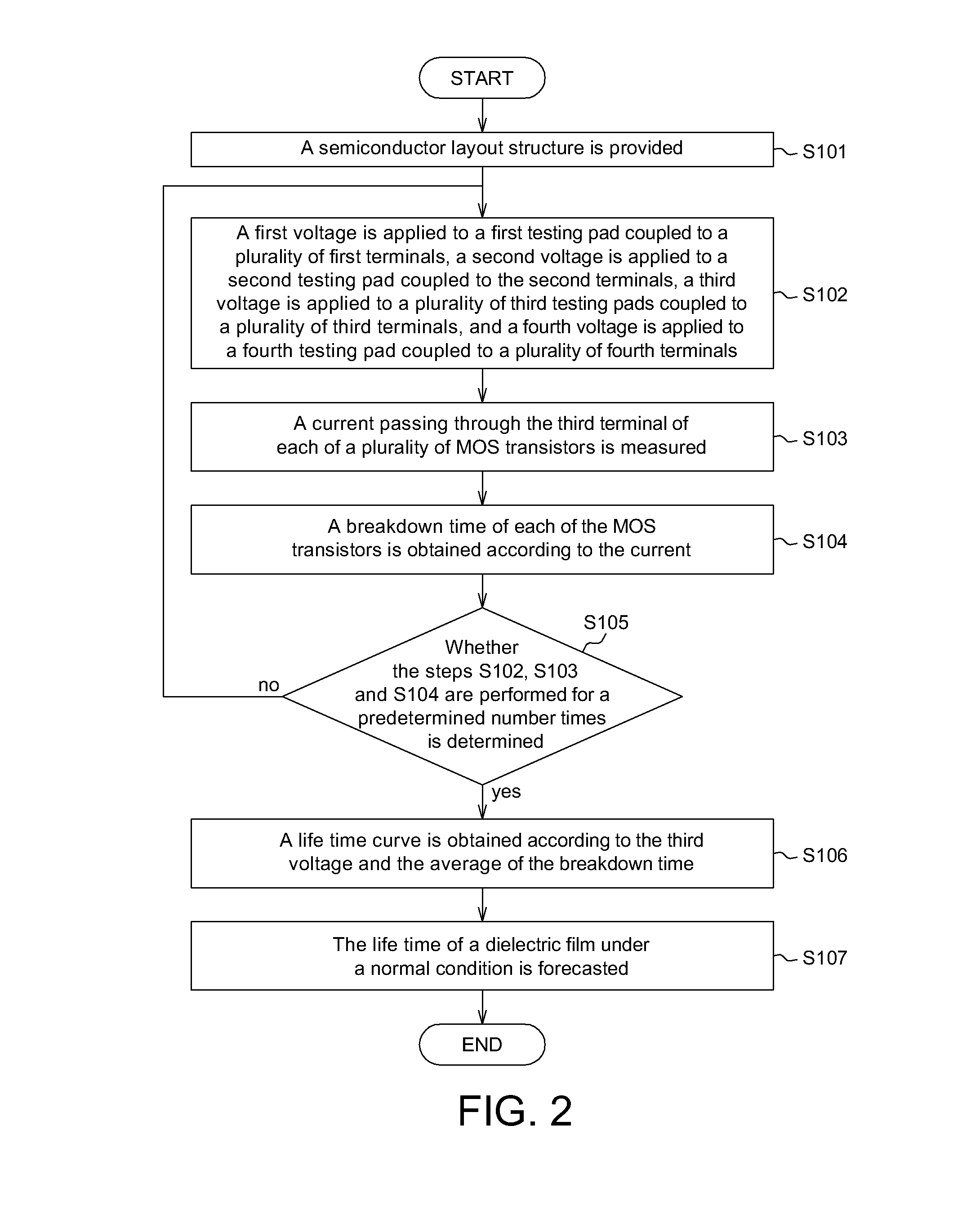
[0016]The semiconductor layout structure 1000 is used for testing the time dependent dielectric breakdown (TDDB). The breakdown time of a dielectric film of the DUT 1900 can be measured under different predetermined specific conditions. Then, the life time of the dielectric film under a normal conditi...


PUM


Abstract

A semiconductor layout structure and a testing method thereof are disclosed. The semiconductor layout structure includes a device under test (DUT), a first testing pad, a second testing pad and a plurality of third testing pads. The DUT includes a plurality of metal-oxide-semiconductor (MOS) transistors. Each of the MOS transistors includes a first terminal, a second terminal and a third terminal. The first testing pad is coupled to the first terminals for being applied a first voltage. The second testing pad is coupled to the second terminals for being applied a second voltage. The third testing pads are respectively coupled to the third testing pads for being applied a third voltage. The third testing pads are electrical insulated from each other. The third voltage is larger than the first voltage and the second voltage.

Description

BACKGROUND OF THE INVENTION[0001]1. Field of the Invention[0002]The invention relates in general to the invention is related to a semiconductor layout structure and a testing method thereof, and more particularly to a semiconductor layout structure including a plurality of metal-oxide-semiconductor (MOS) transistors, and a testing method thereof for testing the MOS transistors.[0003]2. Description of the Related Art[0004]During semiconductor manufacturing process, the performance of a dielectric film should be evaluated by a wafer acceptance test (WAT) after the manufacturing process, in order to confirm the life time of the semiconductor element.[0005]The accuracy of the wafer acceptance test will affect the quality of the semiconductor element. For example, if an error bar of the wafer acceptance test is large, the life time of the semiconductor element cannot be precisely forecasted.SUMMARY OF THE INVENTION[0006]The invention is directed to a semiconductor layout structure and a ...

Claims


Application Information

Patent Timeline
Patent Type & Authority Applications(United States)
IPC IPC(8): G01R31/26
CPCG01R31/2621G01R31/2831G01R31/2858G01R31/2884H01L22/34
Inventor CHANG, CHUN-MINGHOU, CHUN-LIANGLIAO, WEN-JUNG
Owner UNITED MICROELECTRONICS CORP
Why Eureka
Try Eureka