Ball grid array package and process for manufacturing same

Active Publication Date: 2008-05-13
UTAC HEADQUARTERS PTE LTD
View PDF57 Cites 449 Cited by
  • Summary
  • Abstract
  • Description
  • Claims
  • Application Information

AI Technical Summary

Benefits of technology

[0009]Advantageously, solder balls are embedded in the overmold material. The solder balls provide a heat path for heat dissipation from the package. Also, the solder balls in t

Problems solved by technology

However, typical PBGA packages include a convoluted signal path, giving rise to high impedance and an inefficient thermal path which results in low thermal dissipation performance.
Because of the absence of a thermal path away from the semiconductor die 24, thermal dissipation in this package is poor.
This package suffe

Method used


Image

  • Ball grid array package and process for manufacturing same
  • Ball grid array package and process for manufacturing same
  • Ball grid array package and process for manufacturing same

Examples


Example

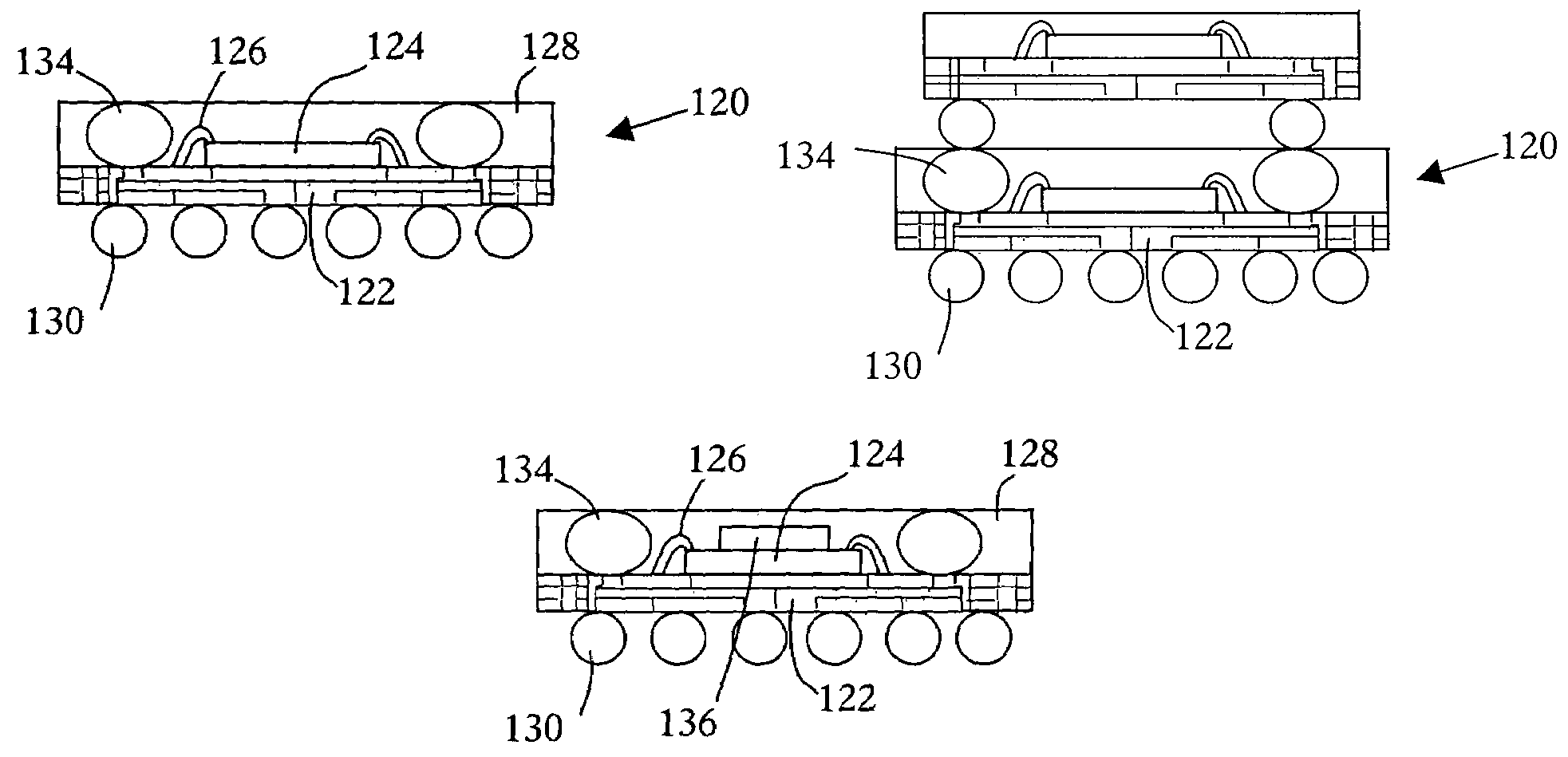
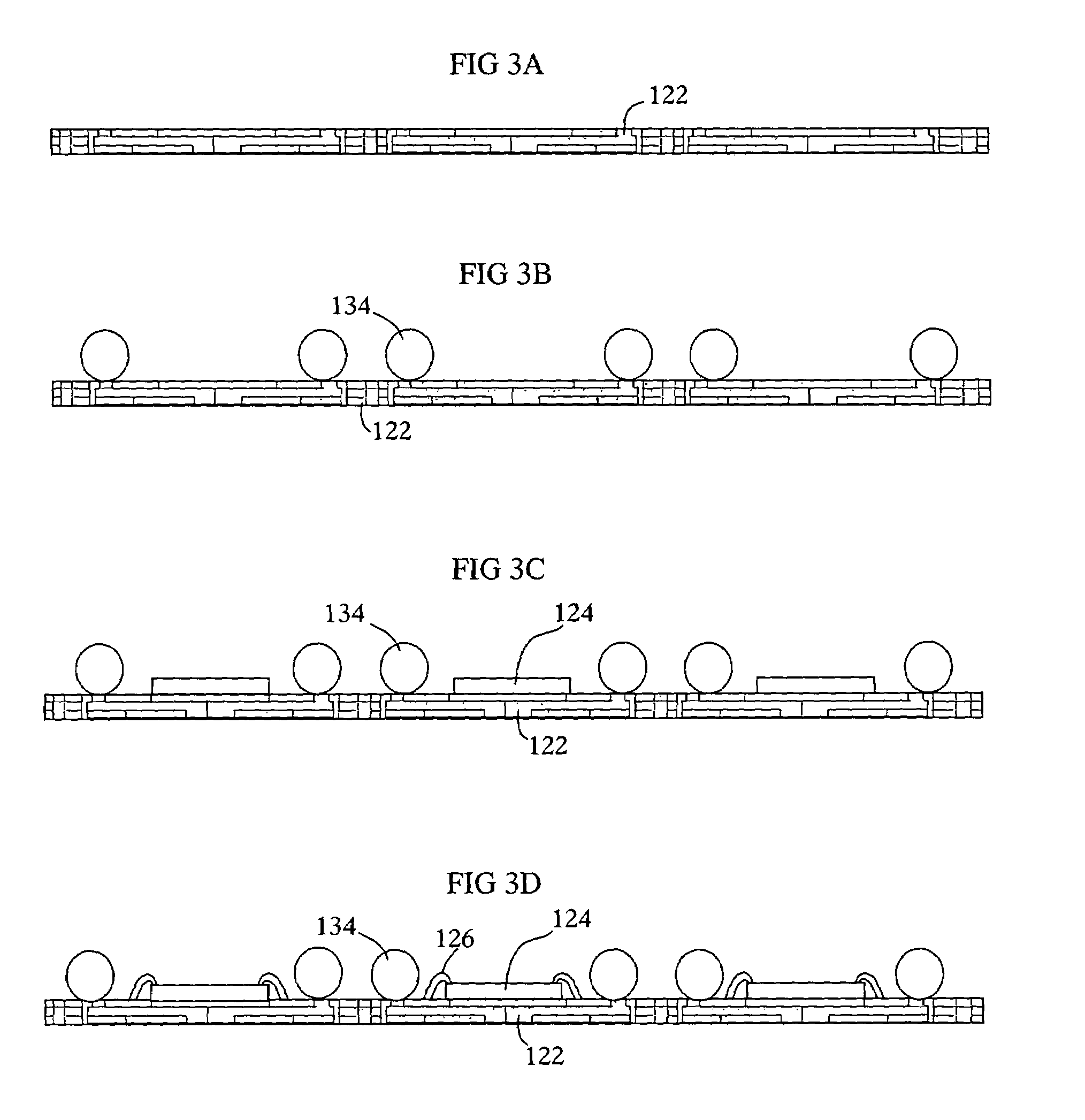
[0021]Reference is now made to FIGS. 3A to 3G to describe a process for manufacturing a ball grid array integrated circuit package, referred to herein as a ball grid array package, according to one embodiment of the present invention. To simplify the description, the numerals used previously in describing FIG. 1 will be used again after raising the numerals by 100 where parts to be described correspond to parts already described.

[0022]Referring to FIG. 3G, the ball grid array (BGA) package is indicated generally by the numeral 120 and includes a substrate 122 having a plurality of conductive traces and a plurality of solder balls 134 disposed on a first surface of the substrate 122. A semiconductor die 124 is mounted to the substrate 122 such that bumps of the semiconductor die 124 are electrically connected to the conductive traces of the substrate 122. An overmold material 128 encapsulates the semiconductor die 124 and the solder balls 134 on the substrate 122 such that portions o...


PUM


Abstract

A process for manufacturing an integrated circuit package includes forming a plurality of solder balls on a first surface of a substrate and mounting a semiconductor die to the substrate such that bumps of the semiconductor die are electrically connected to conductive traces of the substrate. The semiconductor die and the solder balls are encapsulated in an overmold material on the substrate such that portions of the solder balls are exposed. A ball grid array is formed such that bumps of the ball grid array are electrically connected to the conductive traces and the integrated circuit package is singulated.

Description

FIELD OF THE INVENTION[0001]The present invention relates in general to integrated circuit packaging, and in particular to an improved ball grid array package with enhanced thermal characteristics and a unique method of manufacturing.BACKGROUND OF THE INVENTION[0002]High performance integrated circuit (IC) packages are well known in the art. Improvements in IC packages are driven by industry demands for increased thermal and electrical performance and decreased size and cost of manufacture.[0003]In general, array packaging such as Plastic Ball Grid Array (PBGA) packages provide a high density of interconnects relative to the surface area of the package. However, typical PBGA packages include a convoluted signal path, giving rise to high impedance and an inefficient thermal path which results in low thermal dissipation performance. With increasing package density, the spreading of heat generated by the package is increasingly important.[0004]Reference is made to FIG. 1, which shows a...

Claims


Application Information

Patent Timeline
IPC IPC(8): H01L23/48
CPCH01L21/561H01L23/3128H01L23/36H01L23/49816H01L24/97H01L25/105H01L2224/48091H01L2224/97H01L2924/01029H01L2924/01046H01L2924/01047H01L2924/01078H01L2924/01079H01L2924/14H01L2924/1532H01L2924/15331H01L2924/3011H01L2224/85H01L2924/00014H01L2224/81H01L24/48H01L2924/01033H01L2224/73204H01L2224/16225H01L2224/32225H01L2924/00012H01L2224/45144H01L2924/00H01L2225/1023H01L2225/1058H01L2224/48227H01L2224/73265H01L2924/15321H01L24/45H01L24/73H01L2924/00011H01L2924/181H01L2924/00015H01L2224/05599H01L2224/0401
Inventor FAN, CHUN HOMCLELLAN, NEILTSANG, KWOK CHEUNG
Owner UTAC HEADQUARTERS PTE LTD
Why Eureka
Try Eureka