

Device structure and device layout
A device structure and device technology, which is applied in the field of device structure and device layout, can solve the problems of reduced board area, limited reduced area, and limited space, so as to increase battery capacity, reduce the length of wiring, and reduce impedance. Effect
- Summary
- Abstract
- Description
- Claims
- Application Information
AI Technical Summary
Problems solved by technology
Method used
Image

Examples
Embodiment 1
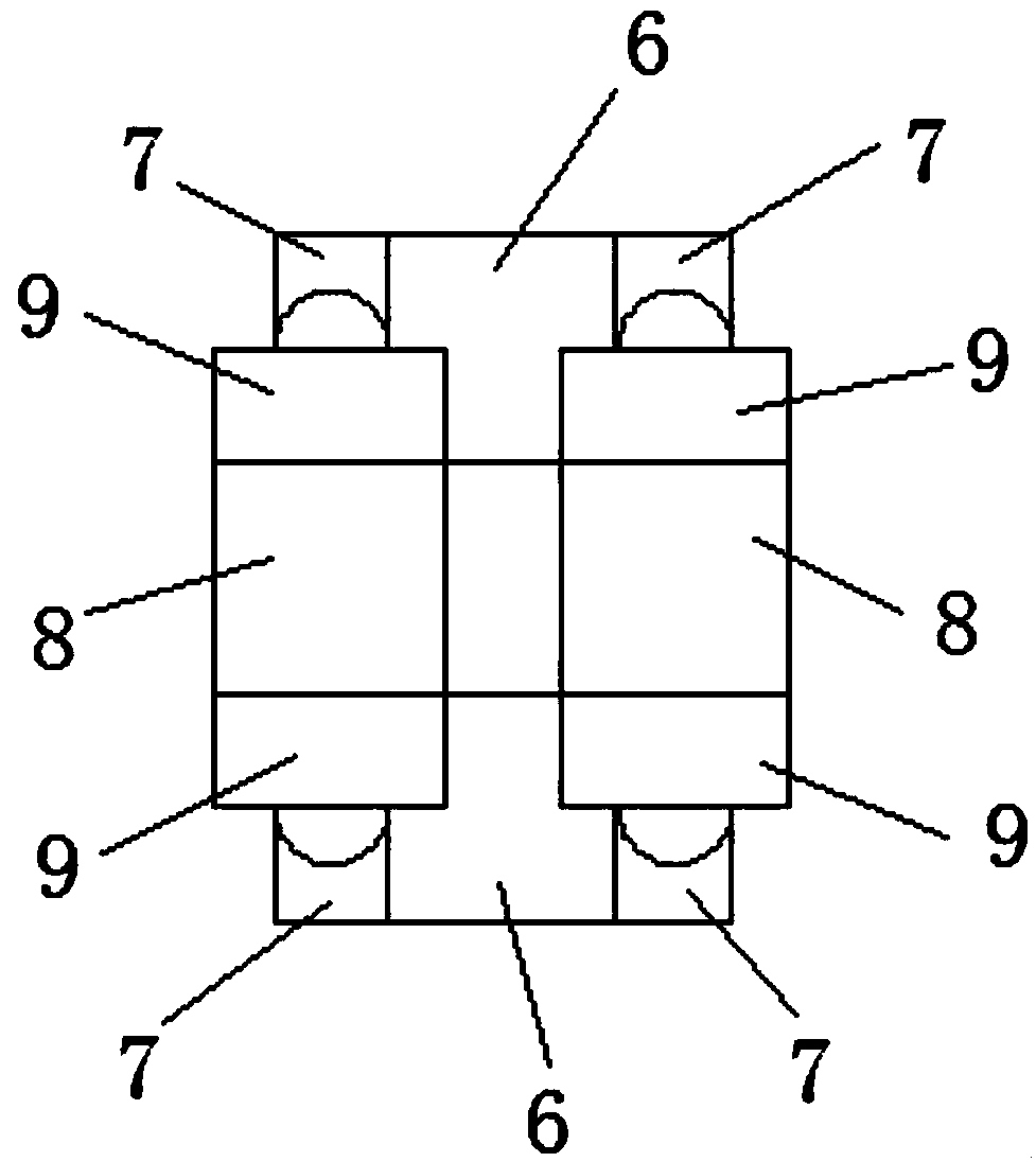
[0050] Such as figure 2 As shown, the device layout structure of the present invention includes two bottom devices 6 and two top devices 8 (the bottom device 6 and the top device 8 are chip devices). Two bottom-layer devices 6 are vertically spaced on the printed circuit board 1, and bottom-layer device soldering terminals 7 are respectively provided at both ends of the bottom-layer device 6; There are top device soldering terminals 9 . The top-layer device welding terminals 9 at both ends of a single top-layer device 8 are respectively welded to the bottom-layer device welding terminals 7 on the same side of the two bottom-layer devices 6 to form a superimposed form.
[0051] Wherein, the distance between the two bottom devices 6 in the longitudinal direction is ≥0.15 mm. The length in the longitudinal direction of the contact surface between the soldering end 9 of the top layer device and the soldering end 7 of the bottom layer device is greater than or equal to 0.2 mm. ...
Embodiment 2
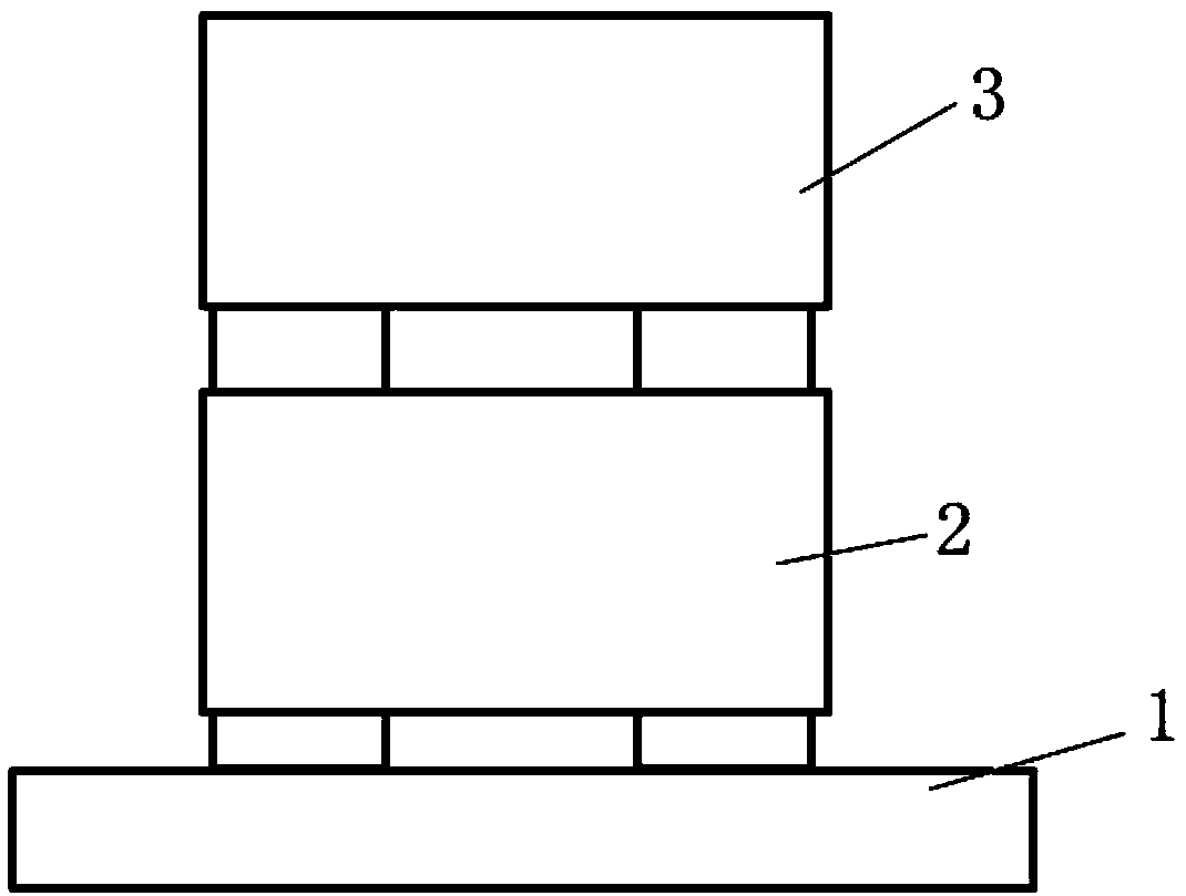
[0053] Such as image 3 , Figure 4 As shown, the device layout structure of the present invention includes a bottom device unit 2 (a QFN device is used in this embodiment), the bottom of the bottom device unit 2 is provided with a bottom solder terminal 10 of the bottom device, and a bottom solder 13 is printed on the printed circuit board 1 , the bottom device unit 2 (a QFN device is used in this embodiment) is pasted on the printed circuit board 1 by soldering the bottom pad 10 of the bottom device and the bottom solder 13 .
[0054] On the opposite side of the bottom device unit 2 (using a QFN device in this embodiment) and the top device unit 3 (using a BGA device in this embodiment), that is, on the top of the bottom device unit 2 (using a QFN device in this embodiment) And the bottom of top layer device unit 3 (adopting BGA device in the present embodiment) is respectively provided with bottom device top welding terminal 11 and top layer device bottom welding terminal 12...
Embodiment 3
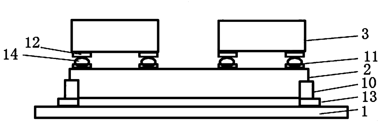
[0056] Such as Figure 5 , Figure 6 As shown, the device layout structure of the present invention comprises a bottom device unit 2 (in this embodiment, a BGA device is used), and the bottom of the bottom device unit 2 is provided with a bottom solder terminal 10 of the bottom device (in this embodiment, a BGA solder ball). Printed circuit board 1 is printed with bottom solder 13, bottom device unit 2 (adopts BGA device in this embodiment) through the soldering of bottom solder 10 (in this embodiment is BGA solder ball) and bottom solder 13 of bottom device unit 2, patch on the printed circuit board 1.
[0057] On the opposite side of the bottom device unit 2 (in this embodiment, a BGA device is used) and the top layer device unit 3 (in this embodiment, a QFN device is used), that is, on the top of the bottom device unit 2 (in this embodiment, a BGA device is used) And the bottom of top layer device unit 3 (adopting QFN device in this embodiment) is respectively provided wi...
PUM
| Property | Measurement | Unit |
|---|---|---|
| Length | aaaaa | aaaaa |
Abstract
Description
Claims
Application Information