
Semiconductor testing apparatus

a technology of semiconductors and testing equipment, applied in electrical testing, measurement devices, instruments, etc., can solve the problems of troublesome adjustment operation and inability of conventional semiconductor testing equipment to adjust the timing of clock signal generation, reduce the effort and time in setting the amount, and reduce the effort and time in actually generating.

Inactive Publication Date: 2008-06-03
ADVANTEST CORP
View PDF2 Cites 8 Cited by
  • Summary
  • Abstract
  • Description
  • Claims
  • Application Information

AI Technical Summary

Benefits of technology

[0007]The present invention is created in view of such a point, and intends to provide semiconductor testing apparatus that can reduce effort to adjust generating timing of a clock signal to be extracted from data or a time required in adjustment.
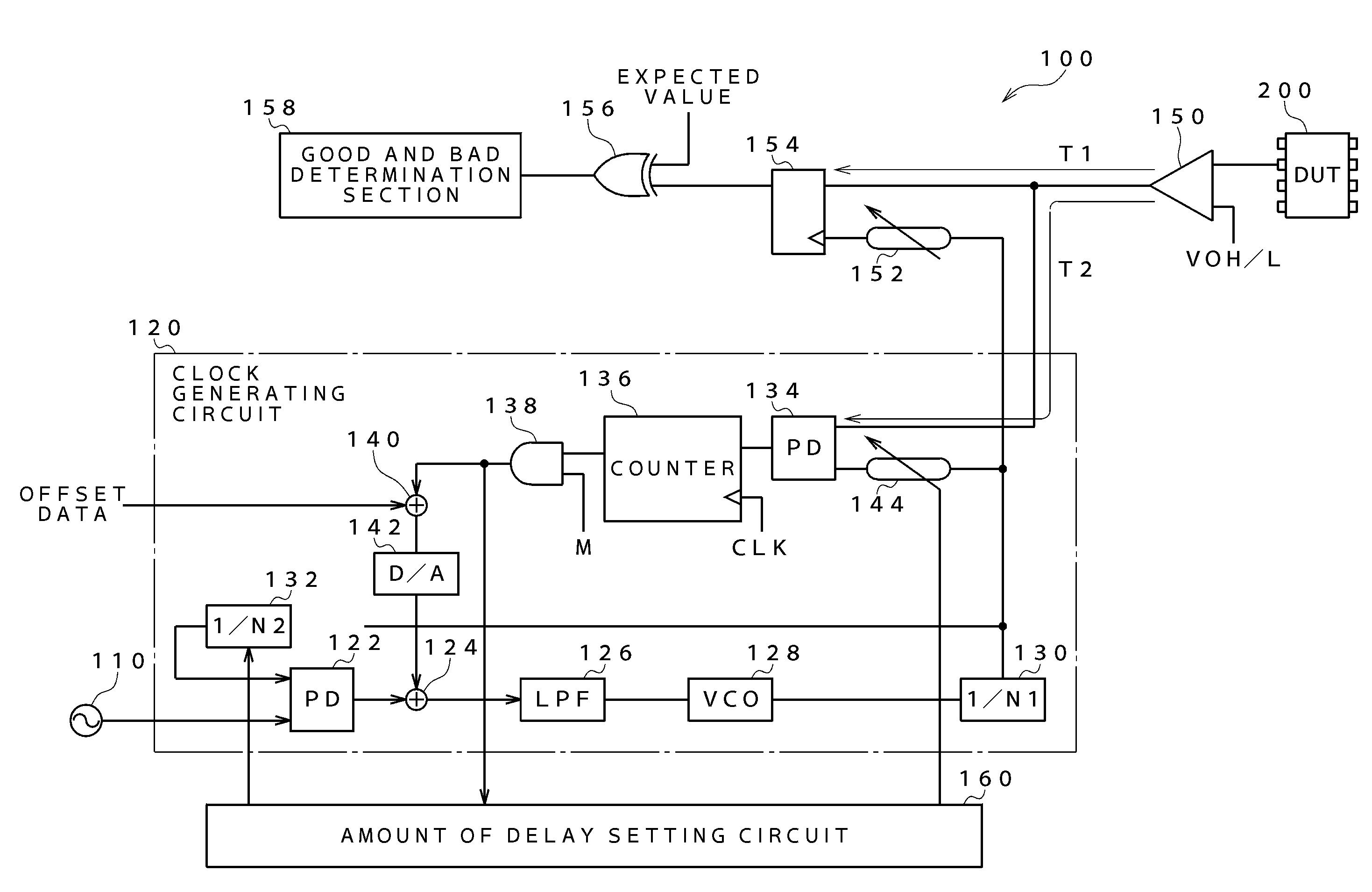
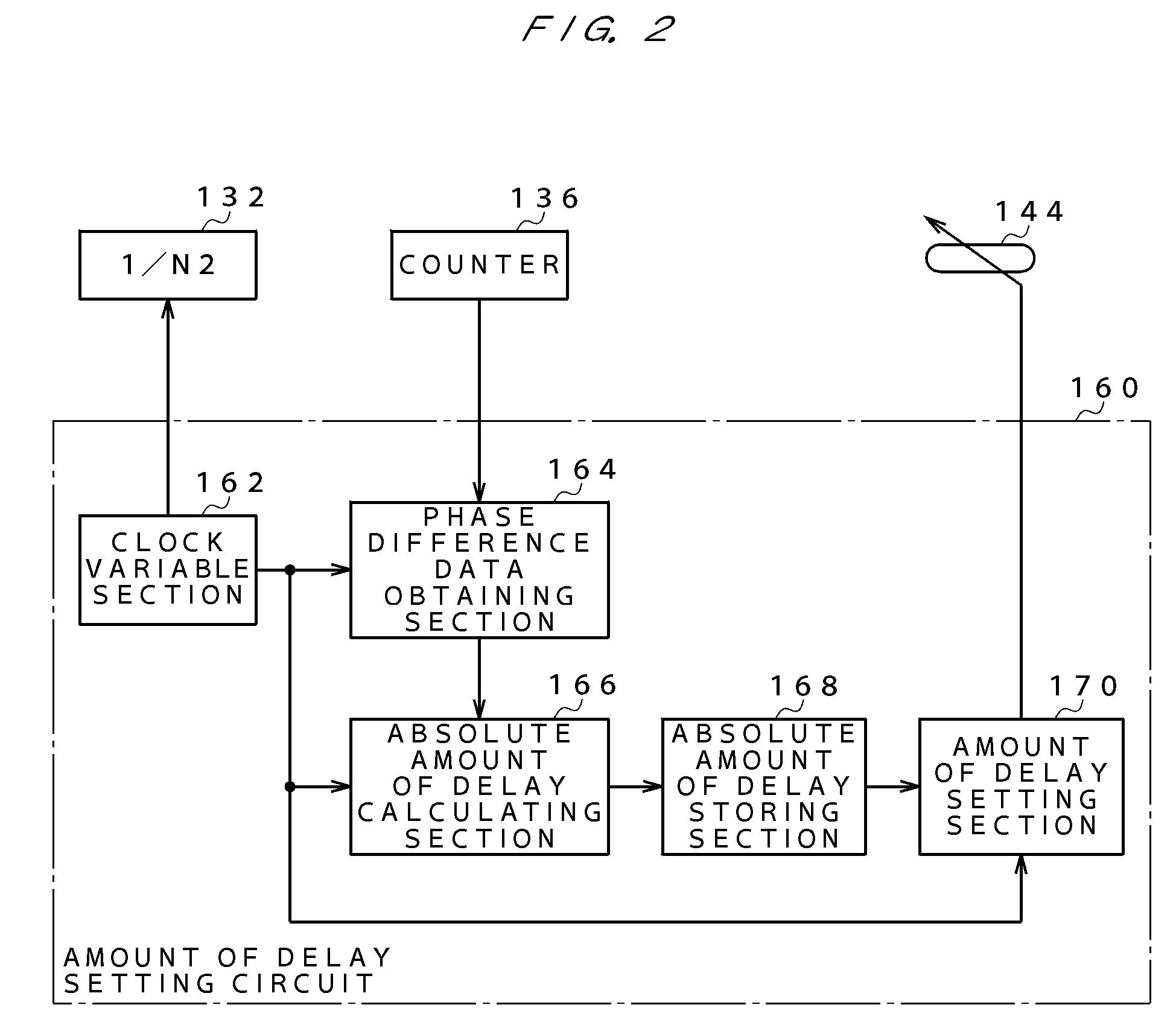
[0008]The semiconductor testing apparatus of the present invention includes a receiving unit for receiving data outputted from a device under test; a clock generating unit for generating a clock signal synchronized with data outputted from the device under test; an absolute amount of delay calculating unit for calculating a signal propagating time corresponding to a difference between a first signal line from the device under test to the receiving unit and a second signal line from the device under test to the clock generating unit as an absolute amount of delay; and an amount of delay setting unit for setting the amount of delay under a period of the clock signal according to a frequency or a period of the clock signal generated by the clock generating unit and ordering adjustment of the clock signal generating timing by the clock generating unit. If the absolute amount of delay can be known, the amount of delay required for adjusting a clock signal generating timing can be known by calculation when a frequency or a period of a clock signal is changed. Therefore, it can substantially reduce effort to adjust clock signal generating timing to be extracted from data or a time required in adjustment.
[0009]It further includes a phase difference data obtaining unit for obtaining a first phase difference data P1 indicating a phase difference between output timing of the data which is generated when a first clock signal having a first frequency or a first period is generated by the clock generating unit and the first clock signal generating timing, and a second phase difference data P2 indicating a phase difference between output timing of the data which is generated when a second clock signal having a second frequency or a second period which is different from the first frequency or the first period is generated by the clock generating unit and the second clock signal generating timing, wherein the absolute amount of delay calculating unit preferably calculates the absolute amount of delay based on the first and second phase difference data P1, P2 obtained by the phase difference data obtaining unit and the first and second frequencies or the first and second periods. The absolute amount of delay can be calculated only when two kinds of clock signals are actually generated and phase difference data is obtained. That can reduce effort and time to actually generate a clock signal and set the amount of delay each time when a frequency or a period of a clock signal is changed thereafter.

Problems solved by technology

The conventional semiconductor testing apparatus mentioned above, however, adjusts variation in a time length of a signal line by assuming that an output timing of data is fixed, it cannot correspond to such a semiconductor device.
That is to say, when output timing of data is shifted due to jitter, generating timing of a strobe signal needs to be shifted by an amount corresponding to the jitter, but conventional semiconductor testing apparatus cannot do such an adjustment.
That makes the adjustment operation troublesome.

Method used


Image

  • Semiconductor testing apparatus
  • Semiconductor testing apparatus
  • Semiconductor testing apparatus

Examples


Embodiment Construction

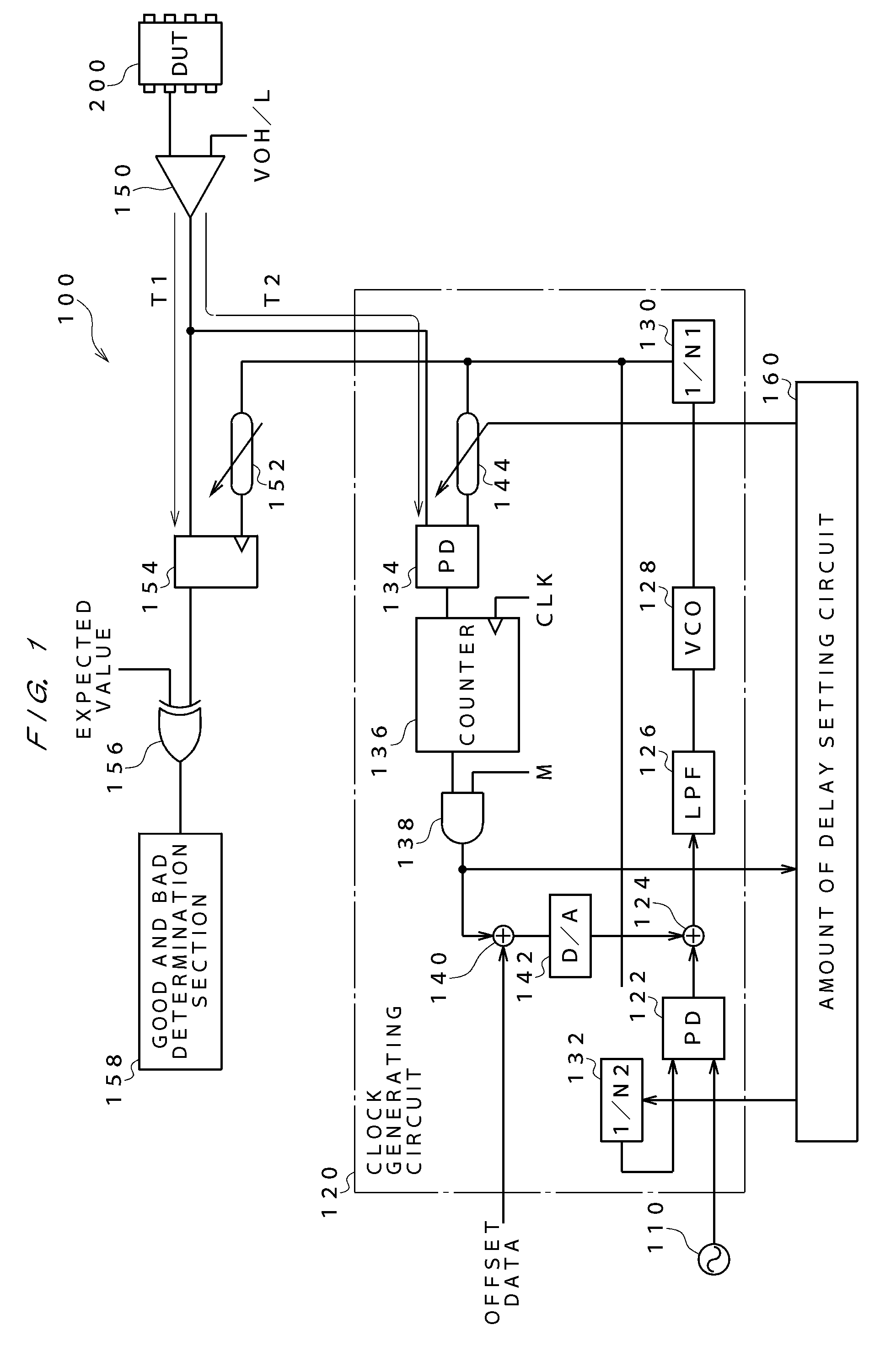
[0019]The semiconductor testing apparatus of an embodiment applied with the present invention will be described below in detail with reference to the drawings. FIG. 1 is a diagram showing a partial configuration of semiconductor testing apparatus of an embodiment. As shown in FIG. 1, a semiconductor testing apparatus 100 of the embodiment includes a reference clock source 110, a clock generating circuit 120, a level comparator 150, a variable delay circuit 152, a timing comparator 154, a logical comparing device 156, a good and bad determination section 158, and an amount of delay setting circuit 160. The good and bad determination unit 158 may be realized by a CPU included in the semiconductor testing apparatus 100 executing a program, or may be realized by using an analyzing device such as a workstation provided outside the semiconductor testing apparatus 100.

[0020]The reference clock source 110 generates a reference clock signal for controlling operation of a device under test (h...


PUM


Abstract

Intends to provide semiconductor testing apparatus that can reduce effort to adjust generating timing of a clock signal to be extracted from data or a time required in adjustment. It includes a timing comparator 154 for receiving data outputted from a DUT 200; a clock generating circuit 120 for generating a clock signal synchronized with data outputted from the DUT 200; an absolute amount of delay calculating unit for calculating a signal propagating time corresponding to a difference between a first signal line from the DUT 200 to the timing comparator 154 and a second signal line to the clock generating circuit 120 as an absolute amount of delay; and an amount of delay setting unit for setting the amount of delay under a period of the clock signal according to a frequency or a period of the clock signal generated by the clock generating circuit 120 and ordering adjustment of the clock signal generating timing by the clock generating circuit 120.

Description

BACKGROUND OF THE INVENTION[0001]1. Field of the Invention[0002]The present invention relates to semiconductor testing apparatus for determining whether a device under test is good or bad based on data outputted from the device under test.[0003]2. Description of the Related Art[0004]Pin electronics of semiconductor testing apparatus includes a comparator which captures a signal outputted from a device under test according to a strobe signal. The comparator does operation of capturing a signal synchronized with a rise (or a fall) of a strobe signal. As a time length of a signal line of each input / output pin of the device under test varies, rise timing of a strobe signal to be inputted into the comparator deviates from expected timing in an initial state. As a result, before various tests are performed on a device under test, timing calibration is performed (for example, see Japanese Patent Laid-Open No. 2-62983). With such timing calibration being performed, influence from variation ...

Claims


Application Information

Patent Timeline
Patent Type & Authority Patents(United States)
IPC IPC(8): G01R31/02
CPCG01R31/31726G01R31/31922
Inventor NEGISHI, TOSHIYUKI
Owner ADVANTEST CORP
Learn More