Vertical-type capacitor structure

a capacitor and vertical-type technology, applied in capacitors, basic electric elements, electric devices, etc., can solve the problems of inconvenient integration of conventional mim capacitors in highly integrated semiconductor devices, inconvenient manufacturing, etc., and achieve the effect of higher integration

Inactive Publication Date: 2008-06-10
COLUMBA TECH INC
View PDF23 Cites 19 Cited by
  • Summary
  • Abstract
  • Description
  • Claims
  • Application Information

AI Technical Summary

Benefits of technology

[0010]The present invention provides a vertical-type capacitor structure, which can be formed by a normal metallization process, and does not require separate capacitor formation processes. The vertical-type capacitor structure occupies a minimum surface area of a semiconductor substrate and thus enables higher integration.

Problems solved by technology

One technique employs an ultra-thin film of dielectric material as a capacitor dielectric layer, but it may incur device reliability problems.
Thus, conventional MIM capacitors are difficult to integrate in highly integrated semiconductor devices.

Method used


Image

  • Vertical-type capacitor structure
  • Vertical-type capacitor structure
  • Vertical-type capacitor structure

Examples


Embodiment Construction

[0020]Reference will now be made in detail to the present embodiments of the invention, examples of which are illustrated in the accompanying drawings. Wherever possible, the same reference numbers will be used throughout the drawings to refer to the same or like parts.

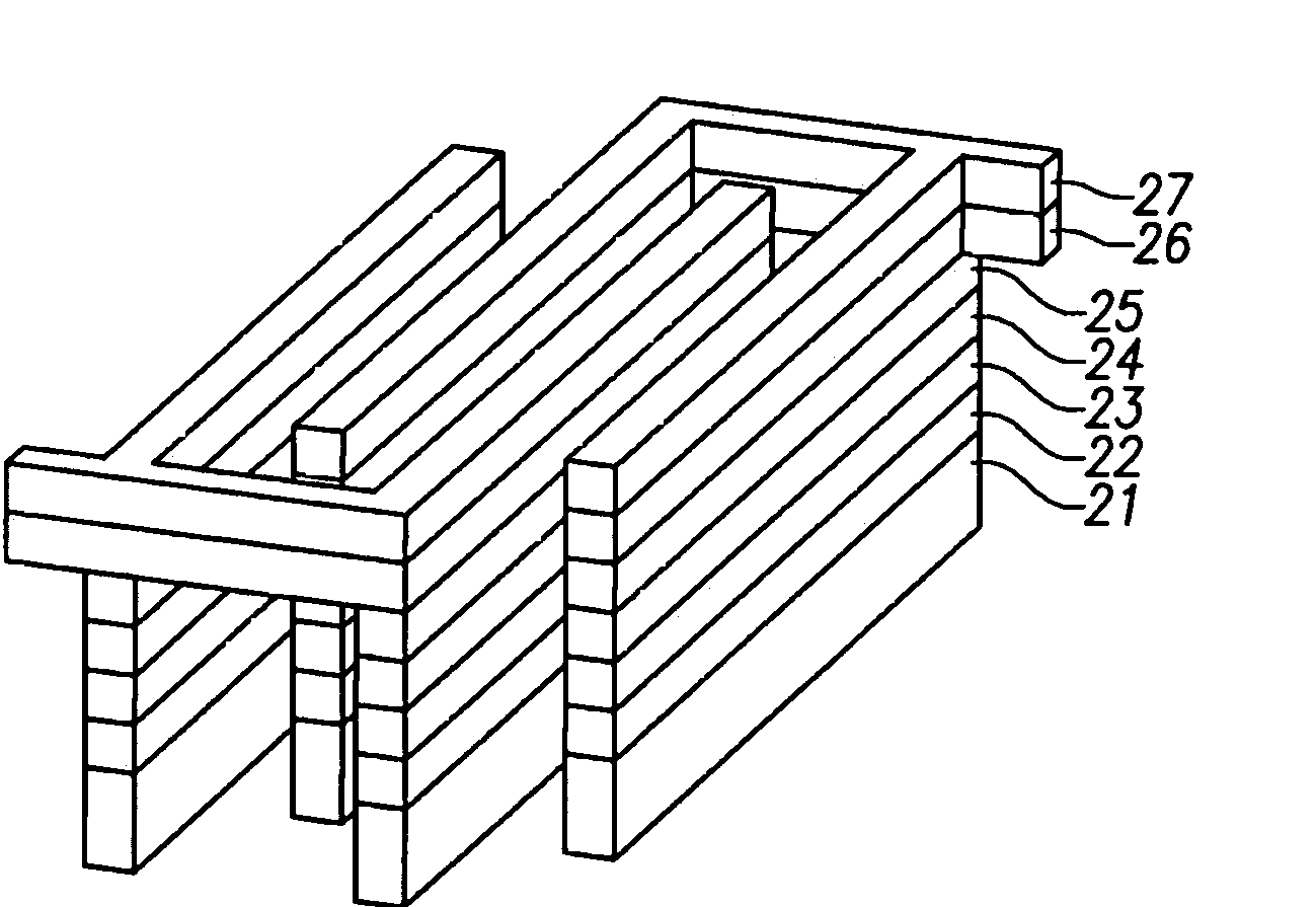
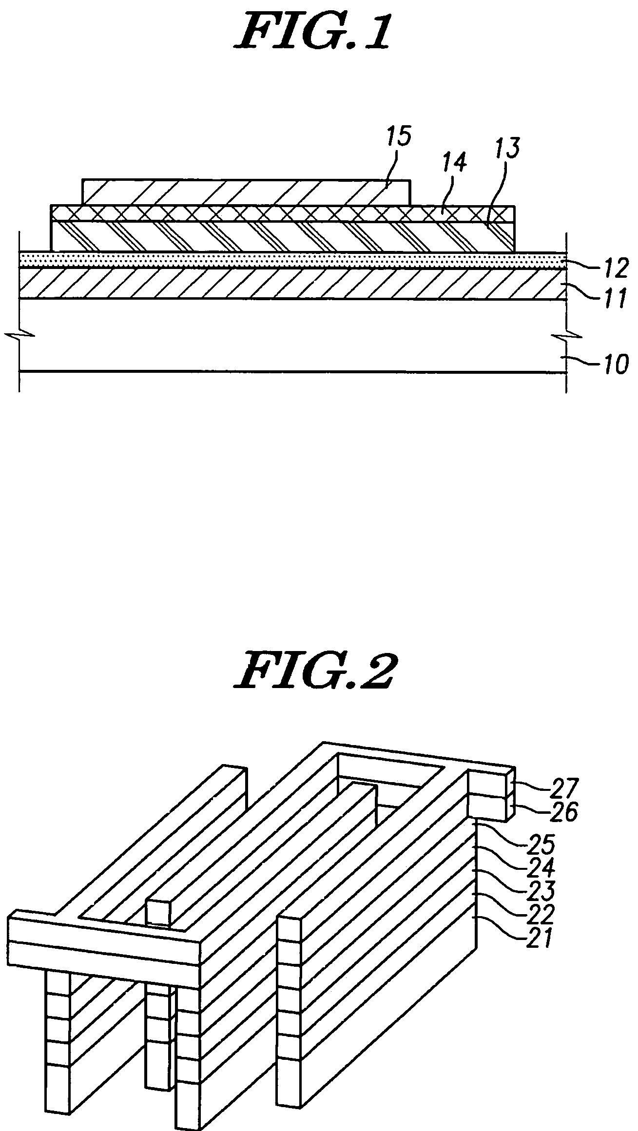
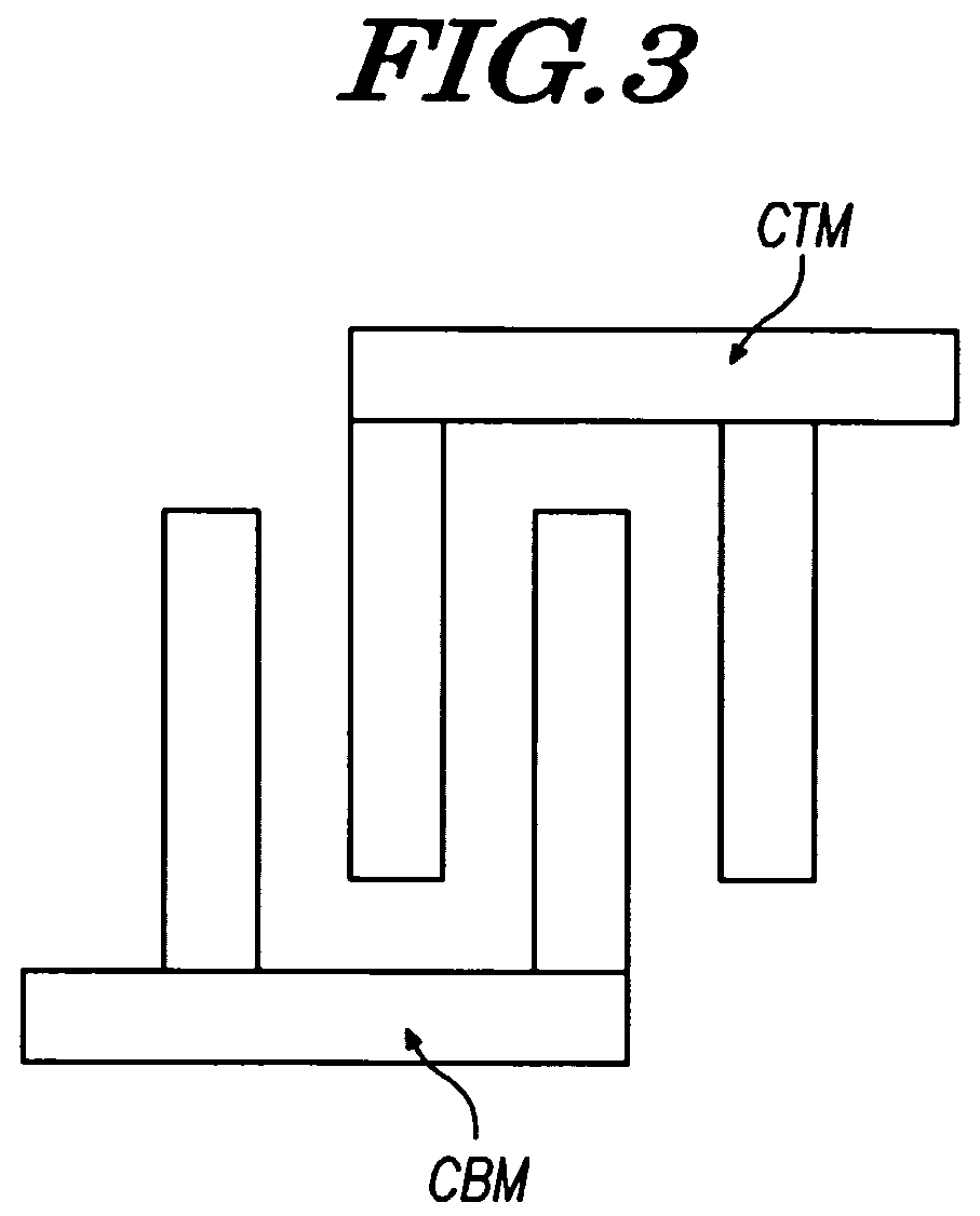
[0021]FIG. 2 is a perspective view of a vertical-type capacitor structure consistent with an embodiment of the present invention, and FIG. 3 is a top view of the vertical-type capacitor structure.

[0022]A first interlevel dielectric layer (not shown) is firstly formed on a semiconductor substrate (not shown). Then, a trench (not shown) is formed in the first interlevel dielectric layer by an etching process. A conductive material, such as copper (Cu), is formed on the first interlevel dielectric layer, filling the trench. Subsequently, the substrate is planarized to remove the conductive material by chemical-mechanical polishing (CMP), retaining a portion of the conductive material to form a first conductive layer 21, ...


PUM


Abstract

Disclosed are a vertical-type capacitor and a formation method thereof. The capacitor includes a first electrode wall and a second electrode wall perpendicular to a semiconductor substrate, and at least one dielectric layer on the substrate to insulate the first electrode wall from the second electrode wall. The first electrode wall includes a plurality of first conductive layers and a plurality of first contacts, the plurality of first conductive layers being interconnected with each other by each of the plurality of first contacts. The second electrode wall includes a plurality of second conductive layers and a plurality of second contacts, the plurality of second conductive layers being interconnected with each other by each of the plurality of second contacts.

Description

[0001]This application claims the benefit of priority of Korean Application No. 10-2004-0114797, filed on Dec. 29, 2004, which is incorporated by reference herein in its entirety.BACKGROUND[0002]1. Technical Field[0003]The present invention generally relates to a semiconductor device manufacturing technology, and particularly to a capacitor structure formed in a semiconductor device, and a fabrication method thereof.[0004]2. Description of the Related Art[0005]A semiconductor device such as an integrated circuit (IC) generally has electronic circuit elements such as transistors, capacitors, and resistors fabricated integrally on a piece of semiconductor material. The various circuit elements are connected through conductive connectors to form a complete circuit that can contain millions of individual circuit elements. In particular, capacitors are used extensively in electronic devices for storing electric charge. Capacitors essentially comprise two conductive plates separated by an...

Claims


Application Information

Patent Timeline
Patent Type & Authority Patents(United States)
IPC IPC(8): H01L29/94H01L27/108H01L29/76H01L31/119
CPCH01L23/5223H01L27/0805H01L28/86H01L2924/0002H01L2924/00H10B12/00
Inventor CHOI, CHEE HONG
Owner COLUMBA TECH INC
Why Eureka
Try Eureka