Reflective liquid crystal display

a liquid crystal display and reflector technology, applied in the field of reflective liquid crystal display, can solve the problems of reducing the numerical aperture, flickering and burning, and light leakage, and achieve the effect of increasing storage capacitance and minimizing light leakag

Active Publication Date: 2008-06-17
JVC KENWOOD CORP A CORP OF JAPAN
View PDF12 Cites 15 Cited by
  • Summary
  • Abstract
  • Description
  • Claims
  • Application Information

AI Technical Summary

Benefits of technology

[0048]An object of the present invention is to provide a reflective LCD that minimizes light leakage to switching elements due to part of read light L made incident to a transparent substrate with the use of at least two layers of light blocking metal films that are formed one upon another between a semiconductor substrate and a reflective pixel electrode with an insulating film being laid on and under each layer of the light blocking metal films. The number of via-hole forming processes needed for the reflective LCD is smaller than that of the related art 2 by one. The thickness of the light blocking insulating film formed between the two light blocking metal films is set to be appropriate for color-image read light. Each switching element formed on the semiconductor substrate of the reflective LCD can have an increased storage capacitance value.
[0053]According to the second aspect, a storage capacitance value of the storage capacitor in each pixel of the first aspect is the sum of a storage capacitance value of a storage capacitor consisting of a diffused capacitor electrode, an insulating film, a capacitor electrode, and a capacitor electrode contact formed on the semiconductor substrate and a storage capacitance value of a storage capacitor consisting of the two layers of the light blocking metal films and the light blocking insulating film formed between the two layers of the light blocking metal films. The second aspect increases a total storage capacitance value, suppresses variation in potential of the reflective pixel electrodes, and prevents flickering and burning.
[0055]According to the third aspect, at least one of the two layers of the light blocking metal films is made of TiN, Ti, or layered TiN / Ti. The third aspect reduces the reflectance of the light blocking metal films to absorb part of read light. Namely, the third aspect can absorb part of read light entering the openings formed between adjacent reflective pixel electrodes.
[0058]According to the fourth aspect, part of color-image read light made incident from the transparent substrate side through the counter electrode to the liquid crystals and penetrated the insulating film adjacent to the reflective pixel electrodes through the openings formed between adjacent reflective pixel electrodes is blocked by the at least two light blocking metal films from reaching the switching elements. The light blocking metal films are formed one upon another between the semiconductor substrate and the reflective pixel electrodes with an insulating film being laid on and under each of the light blocking metal films. The insulating film laid between the two layers of the light blocking metal films is a light blocking insulating film. The thickness of the light blocking insulating film is set to be equal to or thinner than 400 nm which is the wavelength of B (blue) light contained in the color-image read light. Since it is not necessary to use light having wavelengths equal to or shorter than 400 nm that is the wavelength of B (blue) light contained in color-image read light, the fourth aspect can improve the light blocking effect of the light blocking insulating film.
[0061]According to the fifth aspect, part of color-image read light made incident from the transparent substrate side through the counter electrode to the liquid crystals and penetrated the insulating film adjacent to the reflective pixel electrodes through the openings formed between adjacent reflective pixel electrodes is blocked by the at least two light blocking metal films from reaching the switching elements. The light blocking metal films are formed one upon another between the semiconductor substrate and the reflective pixel electrodes with an insulating film being laid on and under each of the light blocking metal films. The insulating film laid between the two layers of the light blocking metal films is a light blocking insulating film made of SiN or SiON. Part of read light entering the openings formed between adjacent reflective pixel electrodes is blocked by the SiN or SiON film having a low reflectance. At the same time, the light blocking insulating film of SiN or SiON formed between the two layers of the light blocking metal films has a high dielectric constant, and together with the two layers of the light blocking metal films, forms a storage capacitor having a large storage capacitance value. Further, the combination of the light blocking insulating film made of SiN or SiON having a high refractive index and the light blocking metal films having light absorbability can improve the light blocking effect.

Problems solved by technology

The transmission LCDs have a drawback that a TFT (thin film transistor) formed in each pixel is unable to serve as a transmission area to transmit light, and therefore, reduces a numerical aperture.
The variation in the potential of the reflective pixel electrode 30 may cause flickering and burning.
Namely, light leakage occurs.

Method used


Image

  • Reflective liquid crystal display
  • Reflective liquid crystal display
  • Reflective liquid crystal display

Examples


first embodiment

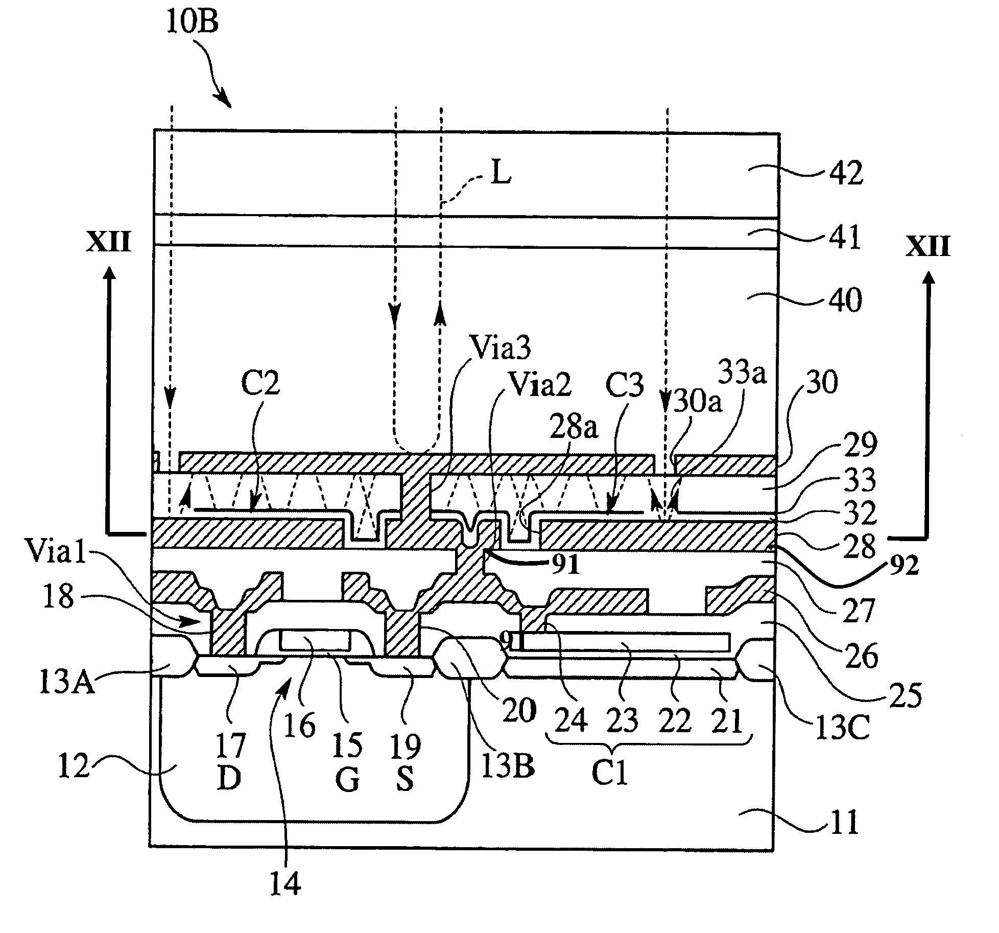
[0078]FIG. 4 is an enlarged sectional view schematically showing a pixel in a reflective LCD according to the first embodiment of the present invention. FIGS. 5A and 5B are enlarged sectional views explaining a third via hole for electrically connecting a first light blocking metal film (second metal film), second light blocking metal film, and reflective pixel electrode (third metal film) shown in FIG. 4 to one another, in which FIG. 5A shows the third via hole filled with tungsten and FIG. 5B the third via hole filled with aluminum wiring. FIG. 6 is a plan view showing the reflective pixel electrode (third metal film), second light blocking metal film, and third via hole shown in FIG. 4. FIGS. 7A and 7B are sectional views explaining the formation of a storage capacitor provided for a switching element in the reflective LCD according to the first embodiment of the present invention, in which FIG. 7A shows the related art 1 as a comparison example and FIG. 7B the present invention....

second embodiment

[0120]FIG. 10 is an enlarged sectional view schematically showing a pixel in a reflective LCD according to the second embodiment of the present invention.

[0121]The reflective LCD 10C according to the second embodiment of the present invention of FIG. 10 is realized by partly changing the locations of the first and second light blocking metal films of the reflective LCD 10B of the first embodiment of the present invention. Only the difference of the second embodiment from the first embodiment will briefly be explained.

[0122]The second embodiment forms no light blocking metal film over a first light blocking metal film (second metal film) 28. Instead, the second embodiment forms a second light blocking metal film 37 over a first metal film 26 with a light blocking insulating film 36 interposed between the films 26 and 37. Due to this, the second embodiment forms the first light blocking metal film 28 over the second light blocking metal film 37 with a second interlayer insulating film...

third embodiment

[0128]FIG. 11 is an enlarged sectional view showing a pixel in a reflective LCD according to the third embodiment of the present invention.

[0129]The reflective LCD 10D according to the third embodiment of the present invention of FIG. 11 is a combination of the light blocking metal films of the reflective LCDs 10B and 10C according to the first and second embodiments of the present invention. Only the difference of the third embodiment from the first and second embodiments will briefly be explained.

[0130]Like the second embodiment, the third embodiment forms a second light blocking metal film 37 over a light blocking insulating film 36 that is formed on a first metal film 26. In addition, like the first embodiment, the third embodiment forms a third light blocking metal film 39 over a light blocking insulating film 38 formed on a first light blocking metal film (second metal film) 28. The third light blocking metal film 39 covers openings 28a formed between adjacent first light bloc...


PUM

PropertyMeasurementUnit
thicknessaaaaaaaaaa
voltageaaaaaaaaaa
wavelengthaaaaaaaaaa

Abstract

A reflective LCD has first and second light blocking metal films that are formed one upon another between a semiconductor substrate and reflective pixel electrodes with an insulating film being laid on and under each of the light blocking metal films, to block part of read light, which has been made incident from a transparent substrate side to liquid crystals through a counter electrode and has penetrated a third interlayer insulating film through openings formed between adjacent ones of the reflective pixel electrodes, from reaching switching elements. One of the first and second light blocking metal films covers the openings formed between adjacent ones of the reflective pixel electrodes. The first and second light blocking metal films in each pixel are electrically connected, through third via holes, to a corresponding switching element, reflective pixel electrode, and storage capacitor.

Description

BACKGROUND OF THE INVENTION[0001]1. Field of the Invention[0002]The present invention relates to a reflective liquid crystal display (LCD), and particularly, to a reflective LCD capable of reducing a leak current produced in switching elements formed on a semiconductor substrate. The leak current is produced when read light that has been emitted to a transparent substrate and made incident to liquid crystals through a counter electrode partly passes through openings formed between adjacent reflective pixel electrodes, penetrates an insulating film adjoining the reflective pixel electrodes, and reaches the switching elements.[0003]2. Description of Related Art[0004]Recently, projection LCDs to display images on large screens are extensively used for, for example, outdoor public displays, control operation displays, and high-resolution image displays conforming to hi-vision broadcast standards and SVGA computer graphics standards.[0005]The projection LCDs are largely classified into t...

Claims


Application Information

Patent Timeline
Patent Type & Authority Patents(United States)
IPC IPC(8): G02F1/1335G02F1/1343G02F1/136G09G3/36G02F1/1362
CPCG02F1/133553G02F1/136209G02F1/136213
Inventor IWASA, TAKAYUKI
Owner JVC KENWOOD CORP A CORP OF JAPAN
Why Eureka
Try Eureka