Image processing method, image processing apparatus and strage medium

Inactive Publication Date: 2008-06-24
CANON KK
View PDF4 Cites 8 Cited by
  • Summary
  • Abstract
  • Description
  • Claims
  • Application Information

AI Technical Summary

Benefits of technology

[0010]The present invention has been made in consideration of the above situat

Problems solved by technology

This is more serious in the case of using a so-called multi-chip sensor in which a plurality of sensor chips are arranged.
Therefore, the reference level of the black signal differs among a plurality of channels, and the difference in luminance level is caused between image regions corresponding to the respective channels, which leads to remarkable deterioration of image quality.

Method used


Image

  • Image processing method, image processing apparatus and strage medium
  • Image processing method, image processing apparatus and strage medium
  • Image processing method, image processing apparatus and strage medium

Examples


first embodiment

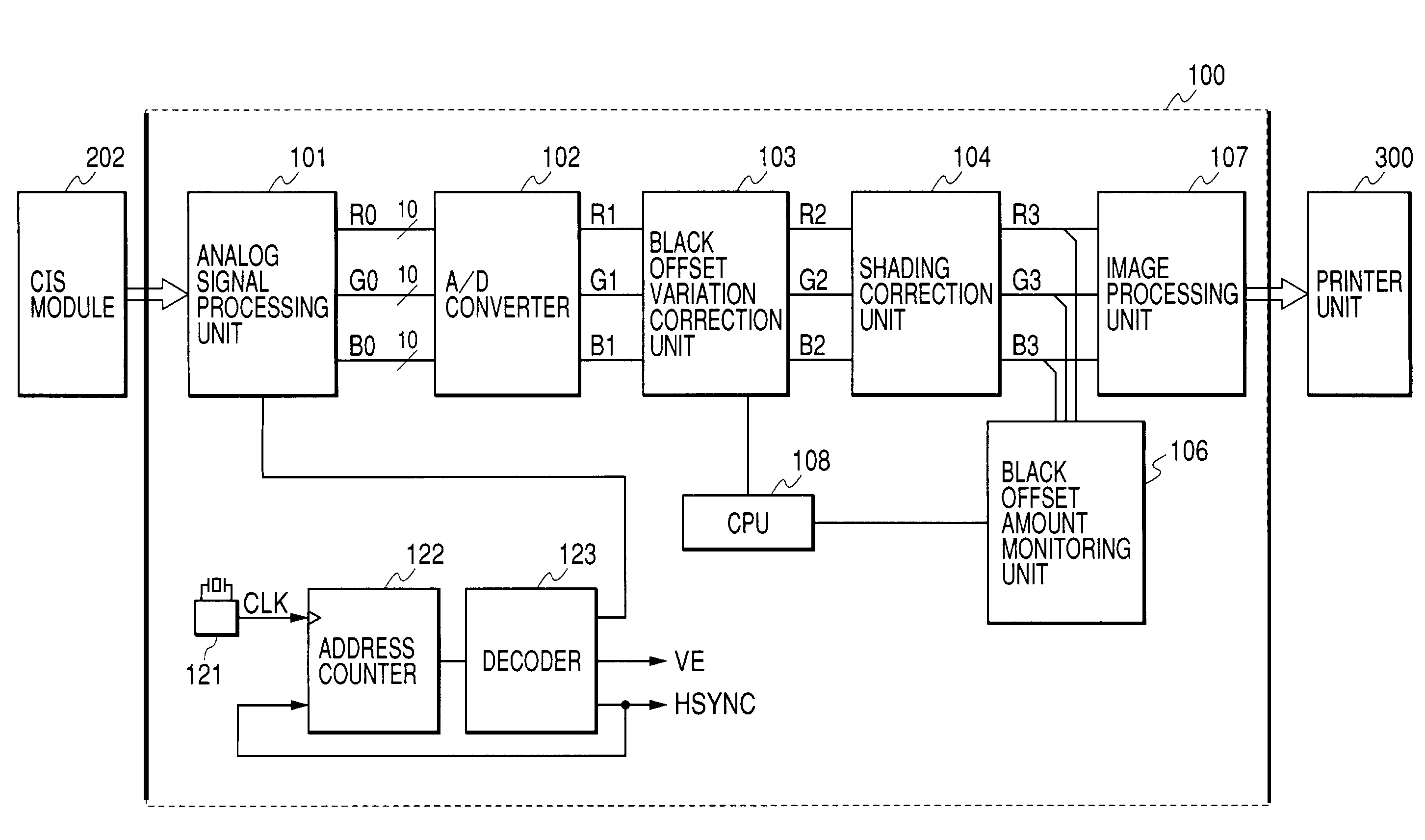
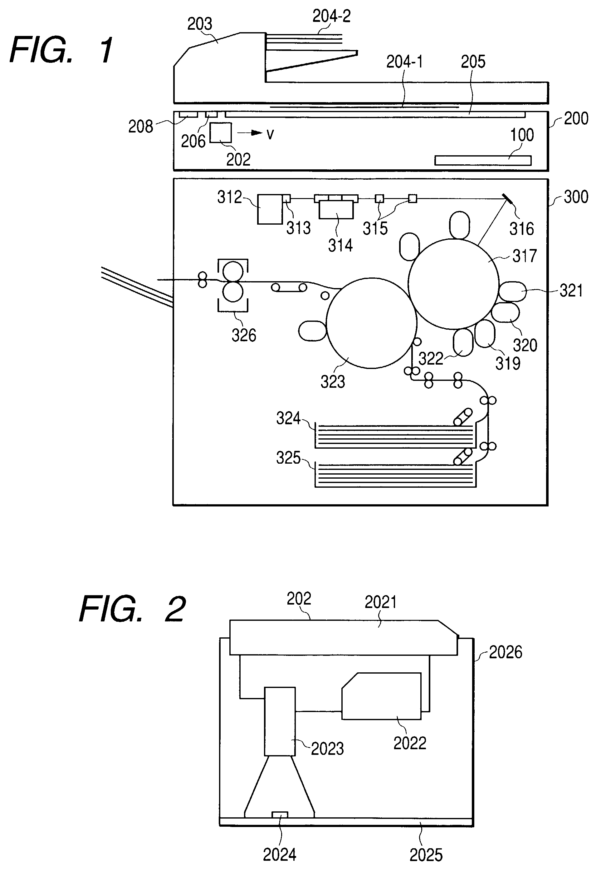
[0033]FIG. 1 is a diagram showing a sectional structure of an image reading apparatus in accordance with an embodiment of the present invention. In the figure, an image scanner unit 200 reads an original as an object, and performs digital signal processing. Further, a printer unit 300 prints out in full color an image corresponding to the image of the original read by the image scanner unit 200 on a sheet.

[0034]A CIS module 202 used in this embodiment will be described with reference to FIG. 2.

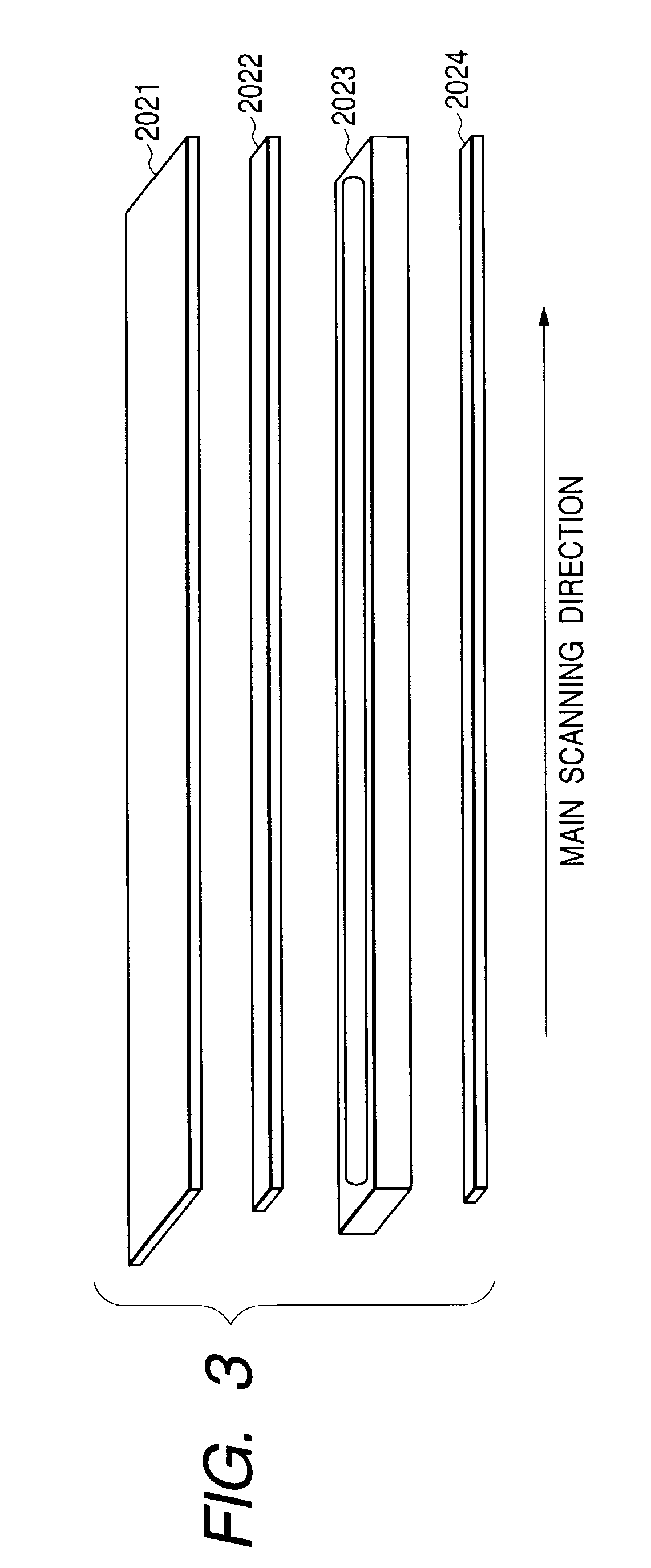
[0035]FIG. 2 is a sectional view taken along a main scanning direction of the CIS module 202 which corresponds to the longitudinal direction. As shown in this figure, the CIS module 202 is structured as follows. That is, a cover glass 2021, an illumination light source 2022 comprised of an LED (light emitting diode), a magnification imaging lens 2023 comprised of a SELFOC lens or the like, and a color line sensor 2024 are mounted onto a substrate 2025, and these are attached to a mold 2026, th...

second embodiment

[0084]There will be described in detail one embodiment in which the image reading apparatus according to the present invention is applied to a sheet feeding apparatus with reference to FIG. 16.

[0085]FIG. 16 is a schematic diagram of an original image reading apparatus for reading an original image in this embodiment.

[0086]Reference numeral 501 denotes a close-contact type image sensor (hereinafter also referred to as CIS), which is constituted by a solid-state image pickup element 502, a SELFOC lens 503, an LED array 504 and a contact glass 505.

[0087]Conveying rollers 506 are arranged in front of and behind the CIS 501, and are used to arrange an original. A contact sheet 507 is used to make the original in contact with the CIS 501. Reference numeral 510 denotes a control circuit, which conducts processing of signals from the CIS 501 and has the same control function as the control unit 108 in the first embodiment.

[0088]An original detection lever 508 is a lever for detecting that a...


PUM


Abstract

An image reading apparatus is provided which includes a contact image sensor comprised of a plurality of sensor chips arranged in series, an analog image processor for processing an analog image signal from the contact image sensor, a unit for conducting black shading correction for each pixel and a unit for conducting white shading correction for each pixel. The image reading apparatus further includes a unit for digitally monitoring a black offset value corresponding to each chip with respect to the signal that has been processed by the analog image processor and a unit for adding and subtracting a black offset variation amount for each chip in the previous stage of the unit for conducting black shading correction for each pixel, and corrects black offset based on an instruction of a control unit.

Description

BACKGROUND OF THE INVENTION[0001]1. Field of the Invention[0002]The present invention relates to an image reading apparatus having a plurality of channels and an image reading method.[0003]2. Related Background Art[0004]Along with the recent progress of a semiconductor process and of production technology, a contact image sensor (CIS) is used in a scanner for consumers because of its characteristics that the cost is inexpensive and it requires only a smaller amount of light from a light source and other characteristics.[0005]A scanner for consumers in recent years has a main scanning period of about 10 to 20 ms while an image reading apparatus, what is called, a copying machine has a main scanning period of about 300 μs, which is two orders of magnitude faster than the scanner.[0006]Here, as one of the problems that arise in the case where the CIS is used in the image reading apparatus with a higher speed by two orders of magnitude, there is variation of a black offset level (which ...

Claims


Application Information

Patent Timeline
IPC IPC(8): H04N1/40H04N1/401
CPCH04N1/401
Inventor HIROMATSU, KENJI
Owner CANON KK
Why Eureka
Try Eureka