Sealing of organic thin-film light-emitting devices

a light-emitting device and organic technology, applied in the manufacture of electric discharge tubes/lamps, electrical devices, electric devices, etc., can solve the problems of increasing costs and complexity, reducing or destroying the utility of flat panel display or flat panel illumination sources utilizing these devices, and reducing or destroying the utility of flat panel illumination sources, so as to achieve the effect of allowing flexibility and further enhancing manufacturing flexibility

Active Publication Date: 2008-07-01
GLOBAL OLED TECH
View PDF4 Cites 26 Cited by
  • Summary
  • Abstract
  • Description
  • Claims
  • Application Information

AI Technical Summary

Benefits of technology

[0011]In accordance with various embodiments, it is an object to produce heat in the bonding material by subjecting it to direct radiation exposure. The energy absorbing material then melts the adjacent portions of both substrate and cover sheets, which flow together to create a welded bond. The invention eliminates the need to pass the directed energy through either the substrate or cover by locating the energy absorbing material along a peripheral side edge of at least one of the substrate or cover. By utilizing an unrestricted path for the applied energy (such as laser, microwave, infrared, conduction, etc), energy absorption or reflection by the substrate or cover plates to be bonded is eliminated. This makes it is possible to use a wider variety of energy sources and wavelengths to supply the required energy to the absorbing material.
[0013]It is still another object to allow flexibility in the manufacturing process by providing the ability to introduce the energy absorbing material to the bond area after the plates have been located in contact with one another. Manufacturing flexibility is further enhanced by the location of the energy absorbing material external to the main surface of the substrate and / or cover plates since this configuration expedites the convection cooling of the system once the weld is completed and introduces the opportunity for conductive cooling.

Problems solved by technology

Exposure to either of these materials results in the rapid degradation and failure of the devices, reducing or destroying the utility of the flat panel display or flat panel illumination source utilizing these devices.
A limitation of this approach is that all known commercially suitable curable adhesive materials provide an inadequate barrier to water vapor, which creates the need to introduce a desiccant between the cover and substrate, increasing costs and complexity.
This approach suffers from the need to create special glass formulations that allow the laser to pass through one glass layer while being absorbed in the second layer.
The special glass formulations add cost and create problems selecting glasses that are compatible with the sealing process, the process for producing the thin-film organic light-emitting devices, and the optical functionality of the completed device.
The method suffers also from the need to leave a margin between the seal and the edge of the cover and substrate glasses.
However, this approach still suffers the same limitations relating to glass formulation, functional compatibility, and edge margin.
While this approach probably creates fewer material compatibility problems, especially in terms of allowing both glass layers to be optically transparent, the method still suffers from limiting material choices.
It also creates a new problem—producing the energy absorbing material in the right shape and thickness to match the spacing requirements of the completed device.
Since the desired gap is typically on the order of 10-20 microns, producing a wire or other form of radiation absorbing material in this thickness or diameter is quite challenging.
Furthermore, the bond width and the spacing between the glass plates can limit the volume of energy absorbing material, and potentially the ultimate bond strength.
This method also introduces a new problem in that the frit is produced from glass and a binder.
In addition, organic thin-film light-emitting devices are very sensitive to contamination, and even after bake-out, the frit will contain small amounts of binder that will be liberated from the frit and trapped in the sealed envelope, risking damage to the encapsulated device.
The main drawback of soldering methods is the cost of solders compatible with glasses, which tends to be high, and the difficulty of controlling the wicking of the solder between the cover and substrate.

Method used


Image

  • Sealing of organic thin-film light-emitting devices
  • Sealing of organic thin-film light-emitting devices
  • Sealing of organic thin-film light-emitting devices

Examples


Embodiment Construction

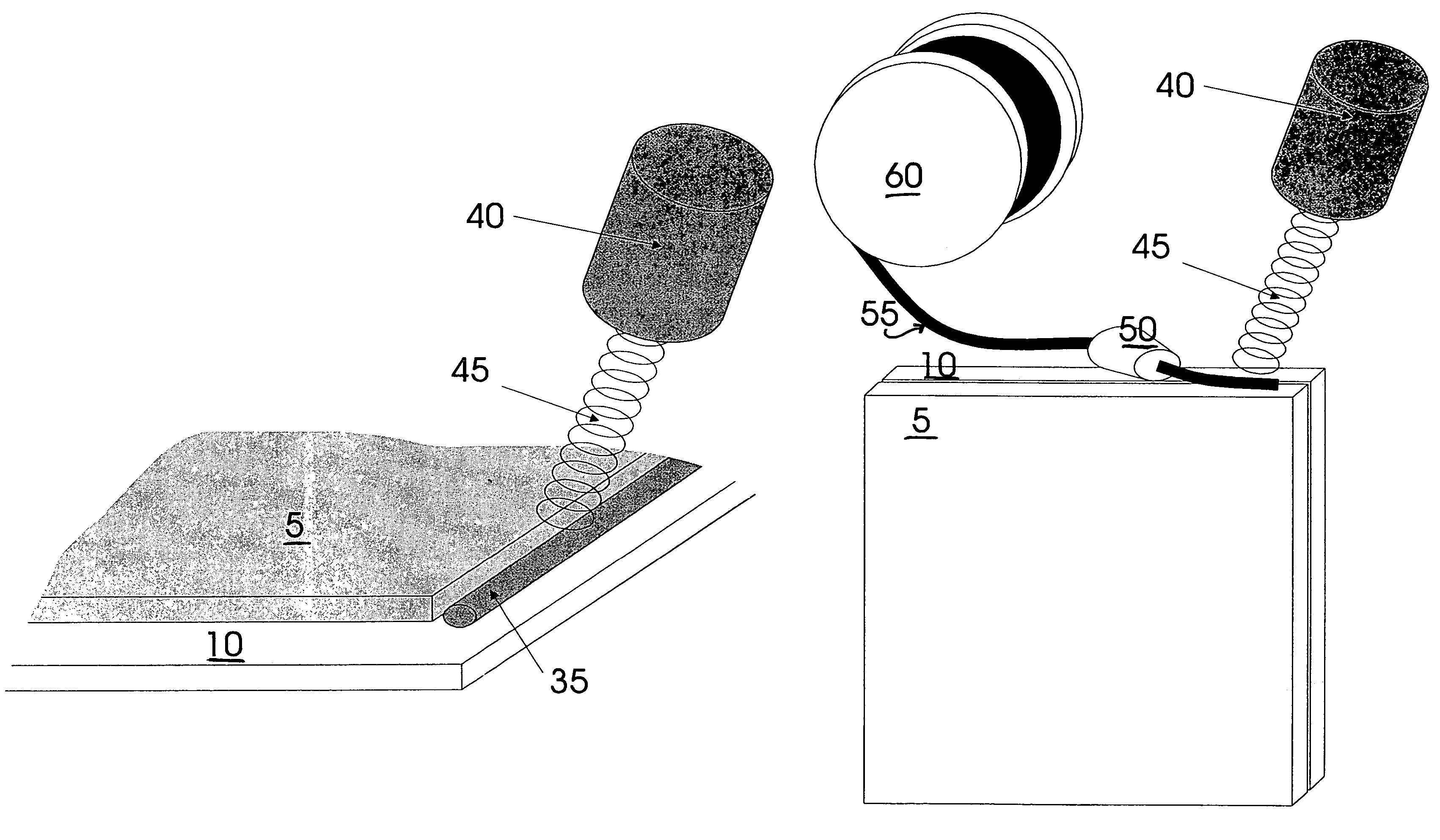
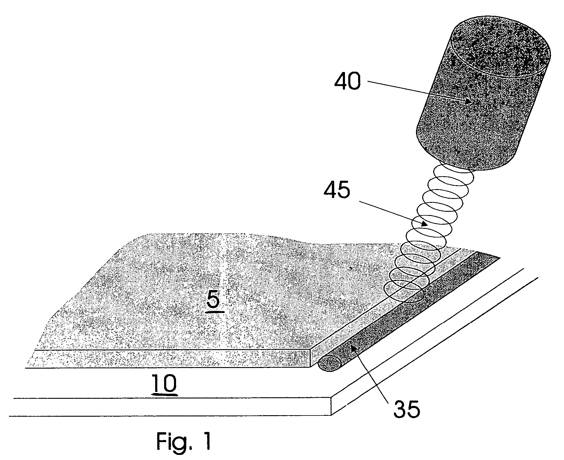
[0021]Referring to FIG. 1, a substrate 10 and a cover 5 are welded together by placing an energy absorbing material 35, shown here as a thin rod or fiber, along the junction of the substrate and cover and directly applying energy to the exposed material 35, shown here as the energy beam 45 from a laser 40. In accordance with one embodiment of the invention, the energy absorbing material is positioned along the peripheral side edge of the cover 5, and also in contact with the adjacent main face of substrate 10. The energy absorbing material gets hot and transfers a portion of the heat to the substrate and cover. The energy is applied until the substrate, cover, and energy absorbing material fuse. Depending on the nature of the energy absorbing material, the substrate and cover may fuse directly, they may each fuse to the energy absorbing material, or the energy absorbing material may diffuse into the cover and substrate, which fuse directly to one another.

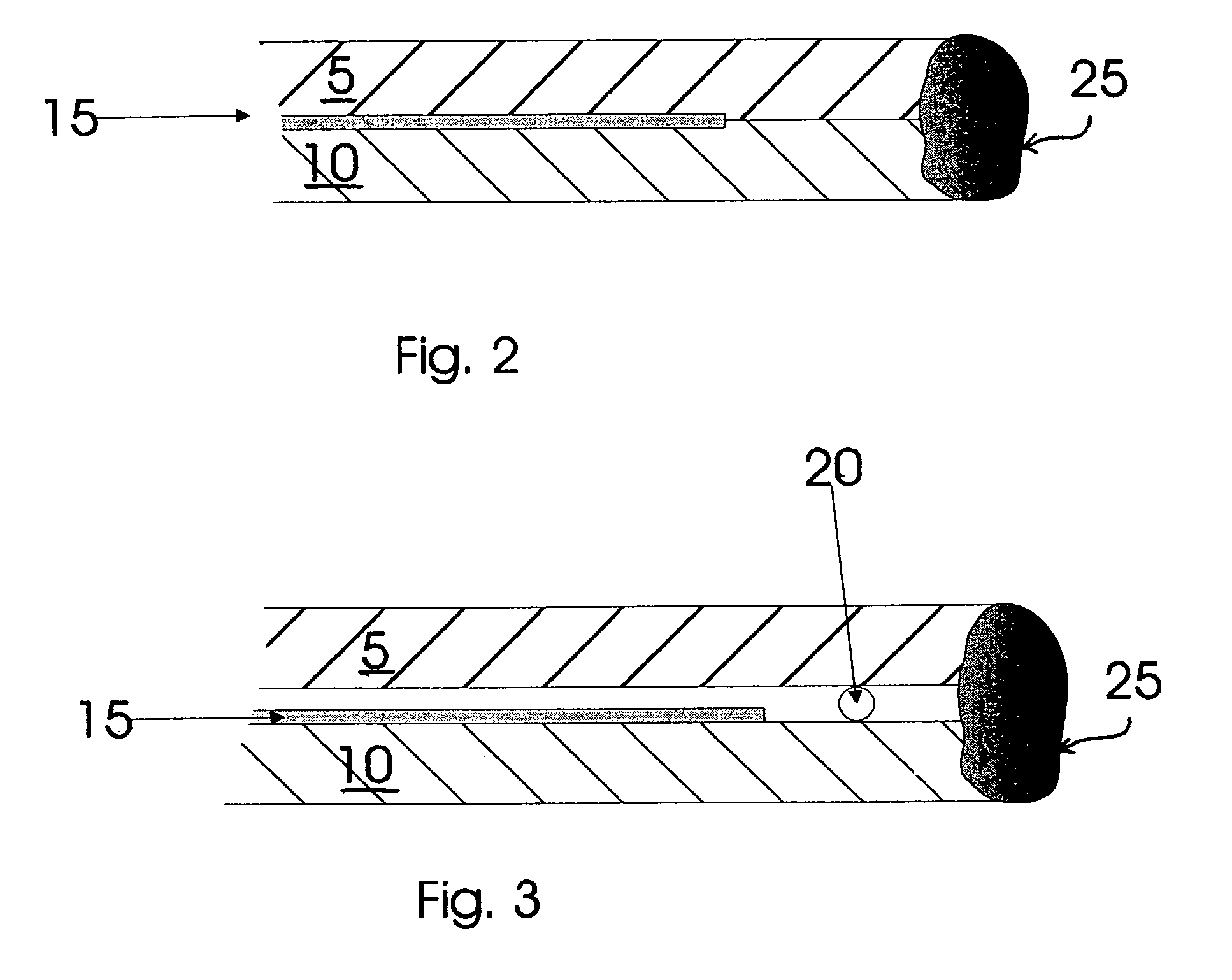
[0022]FIGS. 2-5 illustrate v...


PUM


Abstract

A method for hermetically sealing an organic thin-film light-emitting device between a substrate and a cover including the steps of bringing the substrate and cover into close proximity at a peripheral side edge of at least one of the substrate or cover, bringing an energy absorbing material into contact with the cover and substrate at the peripheral side edge of at least one of the substrate or cover, and applying energy directly to the energy absorbing material, causing the energy absorbing material to transfer heat to the substrate and the cover to fuse and form a hermetic seal along the peripheral side edge.

Description

FIELD OF THE INVENTION[0001]The present invention relates to the sealing of organic thin-film light-emitting devices such as utilized in flat panel displays or flat panel illumination sources constructed on substrates and more particularly to the welding of the substrates to covers.BACKGROUND OF THE INVENTION[0002]Organic thin-film light-emitting devices are known to be exquisitely sensitive to water vapor and oxygen. Exposure to either of these materials results in the rapid degradation and failure of the devices, reducing or destroying the utility of the flat panel display or flat panel illumination source utilizing these devices. A number of approaches have been developed to seal the organic thin-film devices to eliminate exposure to oxygen and water vapor. The most commonly used approach in commercial application is to apply an adhesive between the device substrate and an impermeable cover. A variety of means, such as UV exposure, may be used to accelerate the curing of the adhe...

Claims


Application Information

Patent Timeline
Patent Type & Authority Patents(United States)
IPC IPC(8): H01J9/00
CPCH01L51/5237H10K59/8723H10K59/8722H10K50/8428H10K50/8426
Inventor SPENCER, TIMOTHY F.STRIP, DAVID R.PALONE, THOMAS W.ALLMANN, ERWIN L.
Owner GLOBAL OLED TECH
Why Eureka
Try Eureka