
Flexible circuit substrate for flip-chip-on-flex applications

a flexible circuit substrate and flip-chip technology, applied in the direction of printed circuit, sustainable manufacturing/processing, final product manufacturing, etc., can solve the problem of confined solder bumps of flip-chips on the mounting pad, and achieve the effect of a larger and more uniform standoff distan

Active Publication Date: 2008-07-01
BELL SEMICON LLC
View PDF5 Cites 6 Cited by
  • Summary
  • Abstract
  • Description
  • Claims
  • Application Information

AI Technical Summary

Benefits of technology

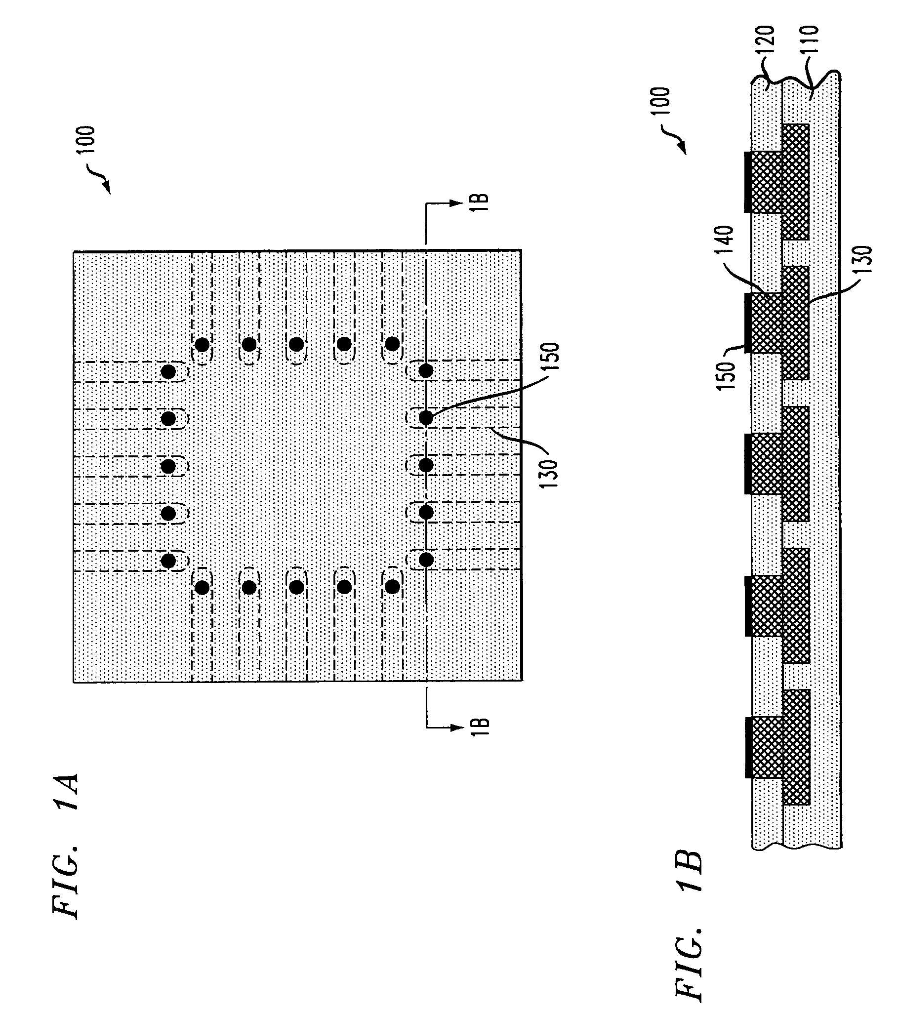
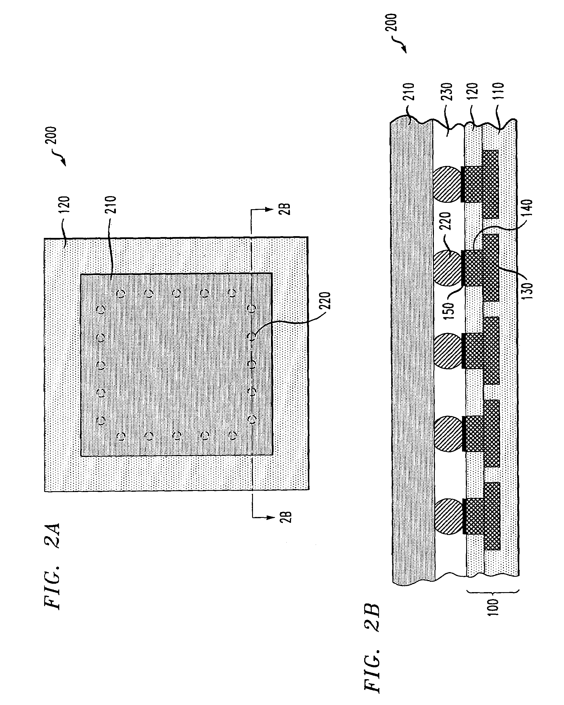
[0007]The present invention addresses the above-identified need by providing an improved flexible circuit substrate for use in FCoF applications. Embodiments of this circuit substrate use mounting pads that are substantially flush with the surface of the flexible circuit substrate. Advantageously, in this way, a larger and more uniform standoff distance is created between the flexible circuit substrate and an attached flip chip when compared to conventional flexible circuit substrates.
[0010]Advantageously, this circuit substrate configuration causes a flip chip's solder bumps to be confined to the mounting pad caps while the flip chip is being attached to the circuit substrate. This confinement limits the collapse of the solder bumps. As a result, the standoff distance between the flip chip and the circuit substrate is more easily maintained within a range that promotes the formation of a complete and uniform layer of underfill material between flip chip and the circuit substrate. A more reliable chip / substrate assembly is thereby formed when using a circuit substrate having features in accordance with aspects of the invention.

Problems solved by technology

Advantageously, this circuit substrate configuration causes a flip chip's solder bumps to be confined to the mounting pad caps while the flip chip is being attached to the circuit substrate.

Method used


Image

  • Flexible circuit substrate for flip-chip-on-flex applications
  • Flexible circuit substrate for flip-chip-on-flex applications
  • Flexible circuit substrate for flip-chip-on-flex applications

Examples


Embodiment Construction

[0018]This invention will be illustrated herein in conjunction with exemplary circuit substrates and methods for forming the exemplary circuit substrates. It should be understood, however, that the invention is not limited to the particular arrangements, materials, film layers and processing steps shown and described herein. Modifications to the illustrative embodiments will become apparent to those skilled in the art.

[0019]Particularly with respect to processing steps, it is emphasized that the descriptions provided herein are not intended to encompass all of the processing steps which may be required to successfully form a functional circuit substrate. Rather, certain processing steps which are conventionally used in forming such circuit substrates, such as cleaning steps, are purposefully not described herein for economy of description. However one skilled in the art will readily recognize those processing steps omitted from this generalized description. Moreover, details of the ...


PUM


Abstract

A circuit substrate for attachment to an integrated circuit chip comprises an electrical trace, a mounting pad and a dielectric layer. The mounting pad has a first surface, one or more sidewalls and a second surface. The first surface is attached to the electrical trace. The dielectric layer substantially covers the one or more sidewalls of the mounting pad and has an uppermost surface that is substantially coplanar with the second surface of the mounting pad.

Description

FIELD OF THE INVENTION[0001]This invention is directed to circuit substrates for integrated circuit chips, embodiments of the invention providing improved flexible circuit substrates for use in flip-chip-on-flex applications.BACKGROUND OF THE INVENTION[0002]Direct chip attachment (DCA) refers to a semiconductor assembly technology wherein an integrated circuit chip is directly mounted on and electrically connected to its final circuit substrate instead of undergoing traditional assembly and packaging. Advantageously, the elimination of conventional device packaging in DCA both simplifies the manufacturing process and reduces the space that the integrated circuit chip occupies on the final circuit substrate. It also improves performance as a result of the shorter interconnection paths between the integrated circuit chip and the circuit substrate.[0003]Flip chip attachment to a flexible circuit substrate (flip-chip-on-flex (FCoF)) is one variant of DCA that is evolving into a mainstre...

Claims


Application Information

Patent Timeline
Patent Type & Authority Patents(United States)
IPC IPC(8): H01L21/44
CPCH01L23/49811H05K1/111H05K3/243H05K3/4007H01L23/4985H01L2224/16225H05K1/0204H05K1/0393H05K3/064H05K3/202H05K3/3452H05K2201/0355H05K2201/0367H05K2201/0376H05K2201/09881H05K2201/10674H05K2203/016H05K1/189H05K2203/0376Y02P70/50H01L23/48
Inventor COHN, CHARLES
Owner BELL SEMICON LLC
Learn More