Nitride semiconductor device and manufacturing method thereof

a semiconductor and nitride technology, applied in the direction of semiconductor devices, basic electric elements, electrical appliances, etc., can solve the problems of drain current decrease, surface fluctuation, etc., and achieve excellent properties, high yield, good reproducibility

Active Publication Date: 2008-04-01
NEW JAPAN RADIO CORP
View PDF2 Cites 4 Cited by
  • Summary
  • Abstract
  • Description
  • Claims
  • Application Information

AI Technical Summary

Benefits of technology

[0004]However, a problem arises in a conventional semiconductor device, where a gate electrode is formed on a nitride semiconductor layer, such as an aluminum gallium nitride (AlGaN) layer or a gallium nitride (GaN) layer, where electrons that have been trapped in the surface level of the nitride semiconductor layer causes the potential of the surface fluctuate, and thereby, a phenomenon (hereinafter referred to as current collapse) where the drain current decreases from the value that has been measured in a quasi-static manner under an operation with a high drain voltage. An object of the present invention is to provide a nitride semiconductor device that can suppress current collapse and a manufacturing method for the same.
[0014]A nitride semiconductor device according to the present invention has a structure where a second nitride semiconductor layer (cap layer) that does not include aluminum is provided on a first nitride semiconductor layer (Schottky layer) with which a control electrode is made to make contact, and the control electrode is formed within a recess that is created by removing a portion of the cap layer through etching, and furthermore, the cap layer has crystallinity with miute grains which have been grown at a temperature lower than the film formation temperature of the Schottky layer and which has high insulation, and therefore, the current collapse is suppressed, through the control of electrons which are trapped in the surface level or through reduction of the surface level density, and thus, high-frequency characteristics are improved.
[0015]Furthermore, in accordance with a manufacturing method for a nitride semiconductor device according to the present invention, a nitride semiconductor device having a desired structure can be formed by controlling the temperature for epitaxial growth in a conventional process for manufacturing a nitride semiconductor device, and therefore, the manufacturing process has good reproducibility, and nitride semiconductor devices having excellent properties can be manufactured with a high yield.

Problems solved by technology

However, a problem arises in a conventional semiconductor device, where a gate electrode is formed on a nitride semiconductor layer, such as an aluminum gallium nitride (AlGaN) layer or a gallium nitride (GaN) layer, where electrons that have been trapped in the surface level of the nitride semiconductor layer causes the potential of the surface fluctuate, and thereby, a phenomenon (hereinafter referred to as current collapse) where the drain current decreases from the value that has been measured in a quasi-static manner under an operation with a high drain voltage.

Method used


Image

  • Nitride semiconductor device and manufacturing method thereof
  • Nitride semiconductor device and manufacturing method thereof
  • Nitride semiconductor device and manufacturing method thereof

Examples


embodiment 1

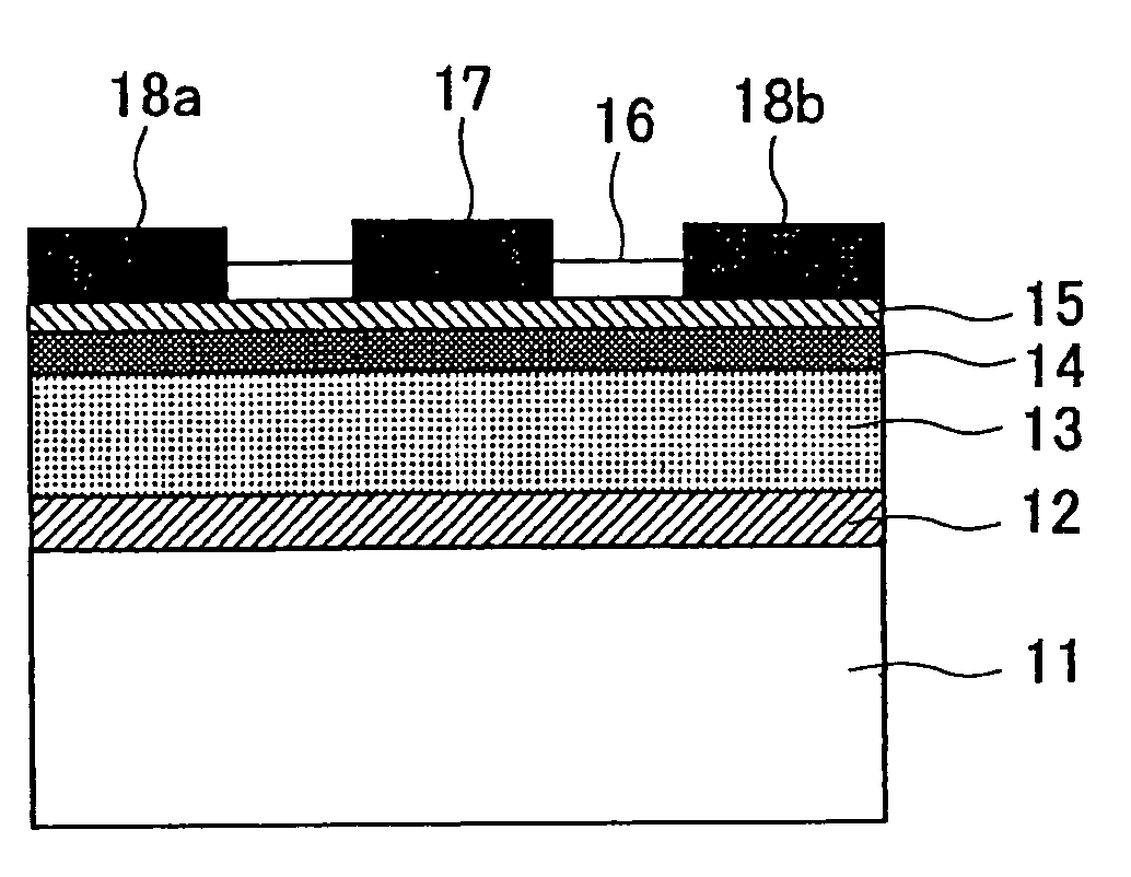
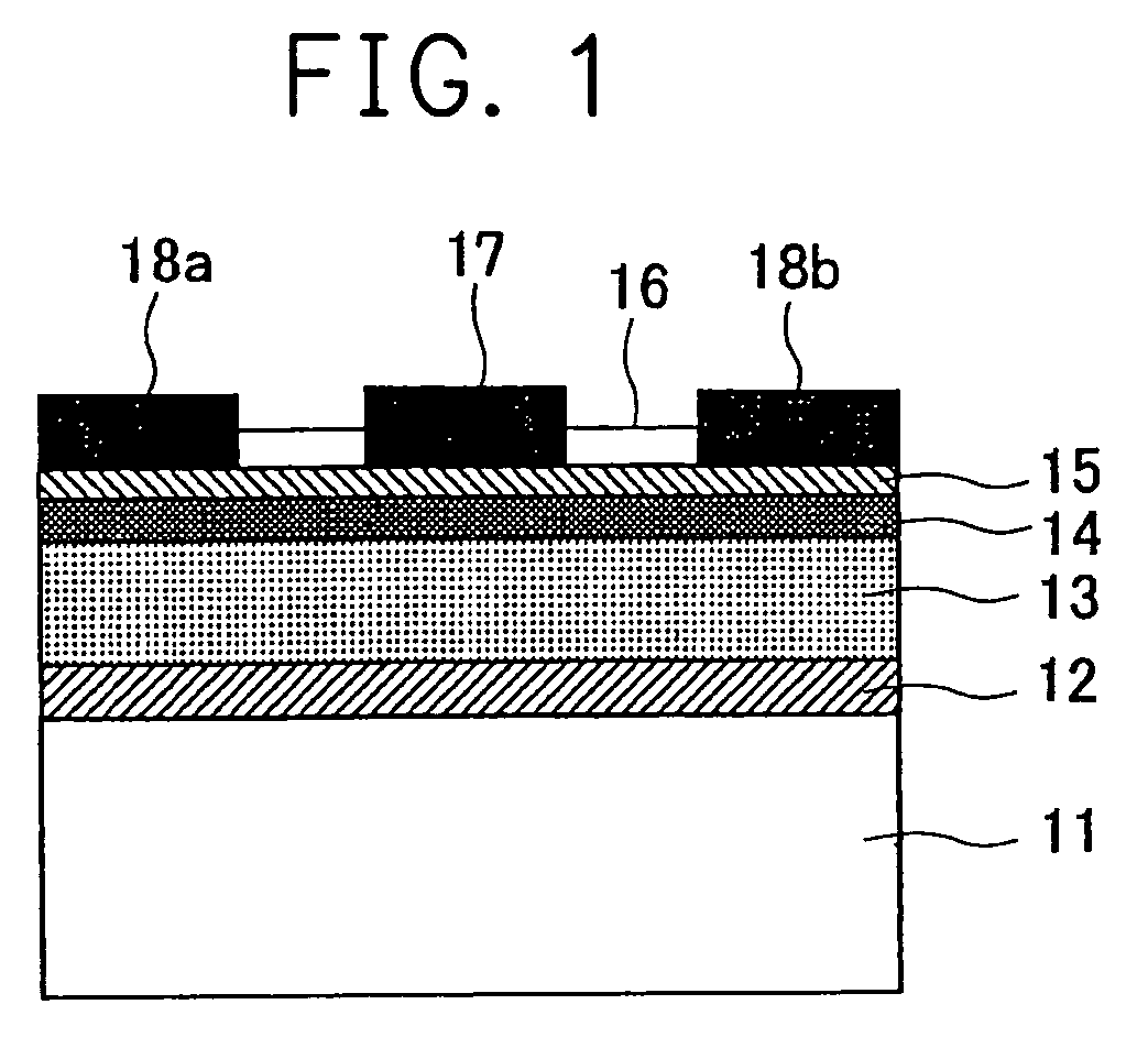
[0023]FIG. 1 is a cross sectional diagram of a HEMT which is a III-V group nitride semiconductor device according to Embodiment 5 of the present invention. As shown in FIG. 1, a buffer layer 12 made of nitride gallium (GaN) and having a thickness of approximately 30 nm, a channel layer 13 having an energy gap that is smaller than the energy gap of the below described charge supply layer, a thickness of 2 μm and made of undoped gallium nitride (GaN), a charge supply layer 14 having a thickness of 15 nm and made of n type aluminum gallium nitride (AlGaN) where a two-dimensional electron gas layer which becomes carriers is formed in the interface between the channel layer 13, and a Schottky layer 15 having a thickness of 3 nm and made of undoped aluminum gallium nitride (AlGaN), and a cap layer 16 having a thickness of 10 nm and made of undoped gallium nitride (GaN) having crystallinity with minute grains are formed and deposited on a substrate 11 made of sapphire. A portion of the cap...

embodiment 2

[0027]Next, a manufacturing method for a HEMT which is a III-V group nitride semiconductor device having the structure shown in the above described Embodiment 2 is cited as an example and a manufacturing method for a nitride semiconductor device according to the present second invention is described.

[0028]First, as shown in FIGS. 5(a) to 5(d), a buffer layer 12 made of gallium nitride (GaN) is grown on a substrate 11 made of sapphire so as to have a thickness of approximately 30 nm in accordance with an MOCVD method, and next, a channel layer 13 made of undoped gallium nitride (GaN) having a thickness of 2 μm, a charge supply layer 14 made of n type aluminum gallium nitride (AlGaN) having a thickness of 15 μm which forms a two-dimensional electron gas layer that becomes carriers in the interface between the channel layer 13 and a Schottky layer 15 made of undoped aluminum gallium nitride (AlGaN) having a thickness of 3 nm are sequentially grown while the temperature of the substrate...


PUM

PropertyMeasurementUnit
thicknessaaaaaaaaaa
thicknessaaaaaaaaaa
thicknessaaaaaaaaaa

Abstract

A nitride semiconductor device enabiling to supress current collapse and manufacturing method thereof including a III-V group nitride semiconductor layer formed of III group elements includes at least one element from the group consisting of gallium, aluminum, boron and indium, and V group elements including at least nitrogen from the group consisting of nitrogen, phosphorous and arsenic, comprising a first nitride semiconductor layer made of said III-V group nitride semiconductor layer deposited on a substrate, a second nitride semiconductor layer comprising said III-V group nitride semiconductor layer and a control electrode making Schottky contact with the first nitride semiconductor layer being exposed through removing a portion of the second semiconductor layer.

Description

BACKGROUND OF THE INVENTION[0001]The present invention relates to a nitride semiconductor device where a nitride semiconductor is used as an active layer and a manufacturing method for the same, and in particular, to a nitride semiconductor device having, a control electrode that makes Schottky contact with the semiconductor device, such as a high electron mobility transistor (HEMT) and a field effect transistor (FET), and a manufacturing method thereof.[0002]FIG. 6 is a cross sectional diagram of a semiconductor device made of a conventional III-V group nitride semiconductor. The semiconductor device shown in FIG. 6 has a so-called HEMT structure where a buffer layer 102 made of gallium nitride (GaN), a channel layer 103 made of gallium nitride, a charge supply layer 104 made of n type aluminum gallium nitride (AlGaN) and a Schottky layer 105 made of undoped aluminum gallium nitride are sequentially deposited on a substrate 101 made of a sapphire substrate, where a two-dimensional ...

Claims


Application Information

Patent Timeline
Patent Type & Authority Patents(United States)
IPC IPC(8): H01L29/739H01L29/24H01L29/812H01L21/335H01L21/338H01L29/20H01L29/778
CPCH01L29/66462H01L29/7787H01L29/2003
Inventor NAKAGAWA, ATSUSHIWAKI, EIJI
Owner NEW JAPAN RADIO CORP
Why Eureka
Try Eureka