Physically highly secure multi-chip assembly

a multi-chip, high-security technology, applied in the field of integrated circuits, can solve the problems of limiting the amount of power consumed inside the device, unable to manufacture all the semiconductor devices that may be needed in the system in a single semiconductor manufacturing process, and unable to fit an entire complex system design

Active Publication Date: 2008-07-22
BEIJING PIANRUOJINGHONG TECH CO LTD
View PDF31 Cites 237 Cited by
  • Summary
  • Abstract
  • Description
  • Claims
  • Application Information

AI Technical Summary

Problems solved by technology

A common problem with building a single chip solution is that often a single chip is too small to fit an entire complex system design in an economic fashion.
Additionally, because of the limits of semiconductor process technologies, all of the semiconductor devices that may be needed in the system may not be able to be fabricated in a single semiconductor manufacturing process.
While an enclosed multi-chip solution alleviates some of the problems of the single chip solution, the use of a fully-enclosed envelope introduces a new set of challenges.
Often these envelopes (and their associated packaging materials) are highly thermally insulative, and thus limit the amount of power that can be consumed inside the device and transmitted through the envelope as heat.
The strict power budget required for such designs often detrimentally impacts the overall performance of the device.
Additionally, because the envelope materials must be as sensitive as possible to potential probing attempts, the reliability problems associated with false positive tampers is significant.

Method used


Image

  • Physically highly secure multi-chip assembly
  • Physically highly secure multi-chip assembly
  • Physically highly secure multi-chip assembly

Examples


Embodiment Construction

[0013]As required, detailed embodiments of the present invention are disclosed herein; however, it is to be understood that the disclosed embodiments are merely exemplary of the invention, which can be embodied in various forms. Therefore, specific structural and functional details disclosed herein are not to be interpreted as limiting, but merely as a basis for the claims and as a representative basis for teaching one skilled in the art to variously employ the present invention in virtually any appropriately detailed structure. Further, the terms and phrases used herein are not intended to be limiting; but rather, to provide an understandable description of the invention.

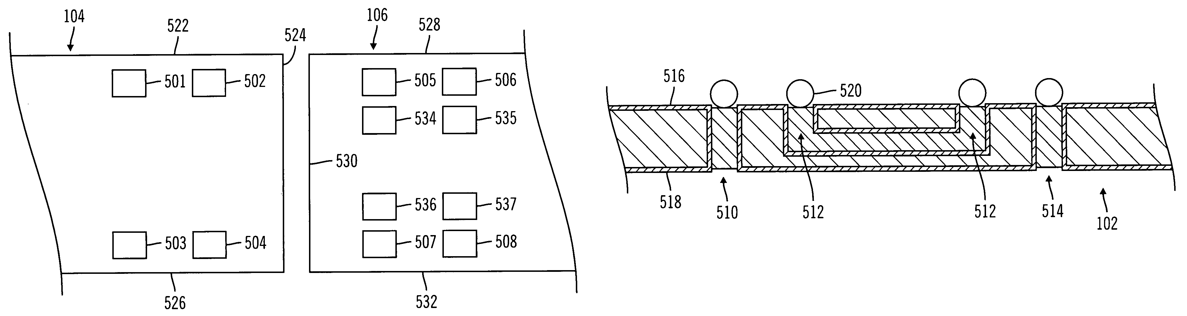
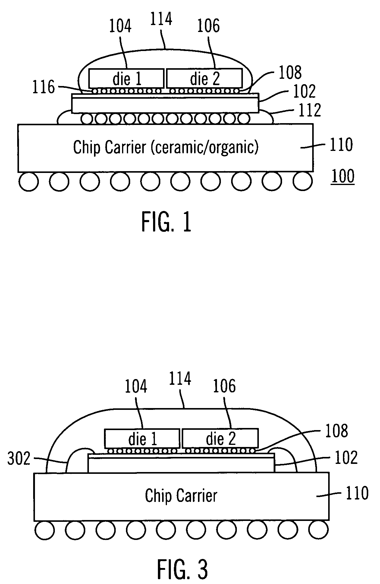
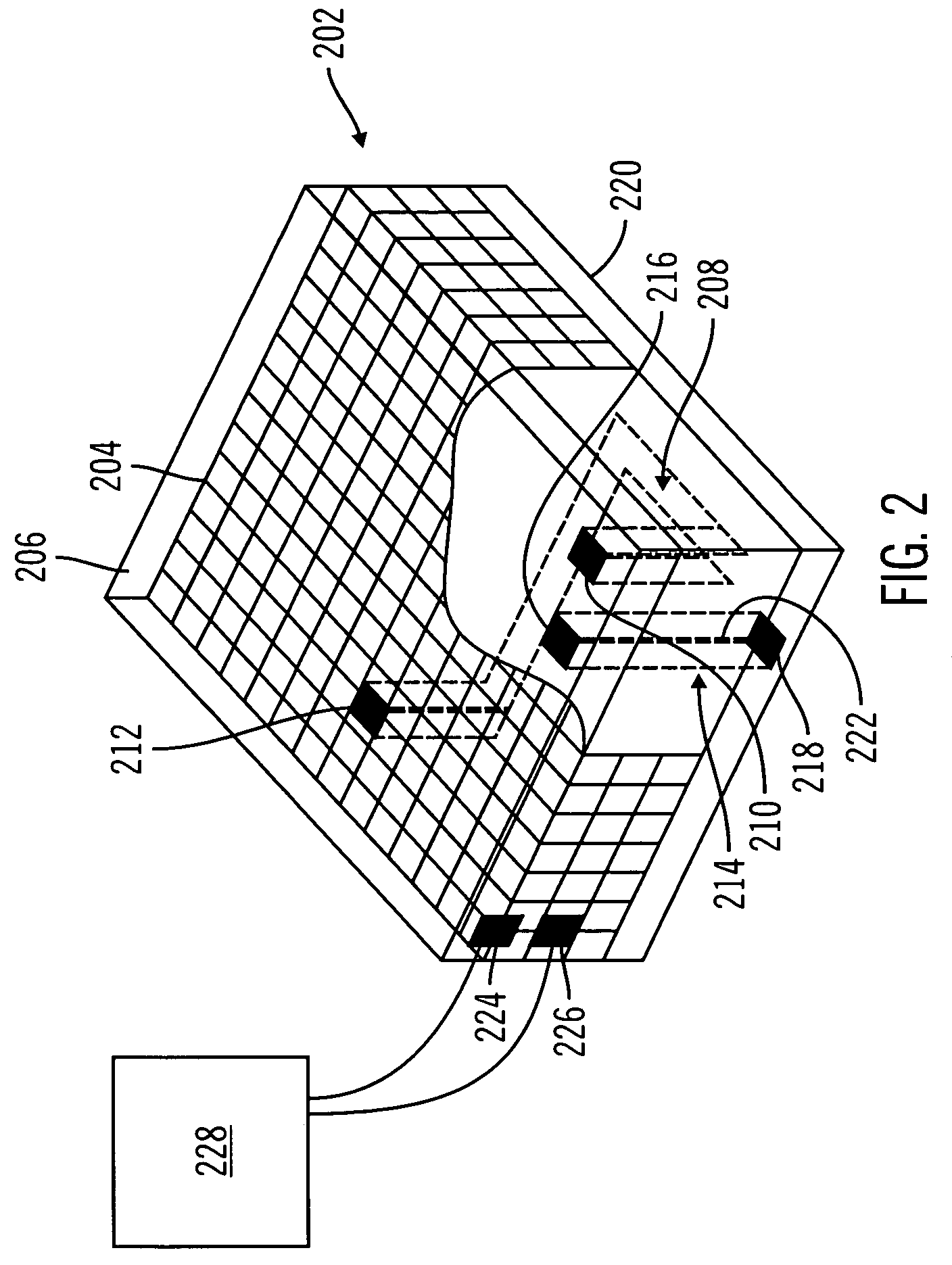
[0014]The present invention, according to a preferred embodiment, provides a physically highly secure multi-chip module without the limitations, such as high temperatures, limited power budgets, and temperamental tamper countermeasures, associated with a conventional secure envelope.

[0015]In accordance with the pri...


PUM

PropertyMeasurementUnit
pressuresaaaaaaaaaa
temperaturesaaaaaaaaaa

Abstract

A physically secure processing assembly is provided that includes dies mounted on a substrate so as to sandwich the electrical contacts of the dies between the dies and the substrate. The substrate is provided with substrate contacts and conductive pathways that are electrically coupled to the die contacts and extend through the substrate. Electrical conductors surround the conductive pathways. A monitoring circuit detects a break in continuity of one or more of the electrical conductors, and preferably renders the assembly inoperable. Preferably, an epoxy encapsulation is provided to prevent probing tools from being able to reach the die or substrate contacts.

Description

FIELD OF THE INVENTION[0001]The present invention relates, in general to integrated circuits, and more particularly relates to computing modules that are physically highly secure against reverse engineering.BACKGROUND OF THE INVENTION[0002]Prevention of reverse engineering and data theft is an important consideration at all levels of computer architecture design. To protect their IP investments, designers currently utilize two main approaches to achieve a physically highly secure computing module. Such a “Highly Secure” computing module is suitable for NIST's FIPS 140-2 level 4 certification for cryptographic modules. The first approach to achieve a physically highly secure computing module is to embody the entirety of a function into a single semiconductor chip whose dimensions are so small that it makes physically probing or optically determining secret information infeasible. The second approach to achieve security is to enclose a set of semiconductor devices (such as a CPU, ASIC...

Claims


Application Information

Patent Timeline
Patent Type & Authority Patents(United States)
IPC IPC(8): H01L23/58B23Q15/00H01L21/00
CPCH01L23/5383H01L23/576Y10T29/53178H01L2224/16H01L2924/01078H01L2924/15311H01L2924/19103H01L2924/19107H01L2224/16225H01L2224/73204H01L2924/10253Y10T29/53052Y10T29/53039H01L2924/00
Inventor CONDORELLI, VINCENZOFEGER, CLAUDIUSGOTZE, KEVIN C.HADZIC, NIHADKNICKERBOCKER, JOHN U.SPROGIS, EDMUND J.
Owner BEIJING PIANRUOJINGHONG TECH CO LTD
Why Eureka
Try Eureka