Apparatus and method of measuring defects in an ion implanted wafer by heating the wafer to a treatment temperature and time to substantially stabilize interstitial defect migration while leaving the vacancy defects substantially unaltered.

a technology of ion implanted wafers and apparatus, which is applied in the field of apparatus and method of measuring defects in an ion implanted wafer, can solve the problems of process not removing vacancy defects and and achieve the effect of improving the sensitivity of currently available instruments and accelerating the migration of interstitial defects

Inactive Publication Date: 2008-07-22
SEMILAB SEMICON PHYSICS LAB
View PDF12 Cites 3 Cited by
  • Summary
  • Abstract
  • Description
  • Claims
  • Application Information

AI Technical Summary

Benefits of technology

[0008]In part, the invention relates to a multi-mode, electro-optical metrology system that improves the sensitivity of currently available instruments. Improvements include a combination of non-contact, real-time, inline, measurements over an extended process space. In particular, a low temperature thermal treatment is described that can be added to an existing metrology system. This thermal treatment accelerates the migration of interstitial defects before measurement commences; however, the process does not remove the vacancy defects that are of interest to the process engineer.
[0009]Furthermore, the low temperature heat treatment has special advantages when applied to multiple wafers. Because of the heat exposure, the interstitial defects in each wafer are stabilized to approximately the same level. Application of the heat treatment prevents each wafer from exhibiting skewed individual capacitive measurements due to interstitial variations. Thus, by using the disclosed low temperature technique on a group of wafers, a relative comparison of the individual measurements is possible. This comparison is feasible due to the standardized interstitial defect baseline that results from the heating process.

Problems solved by technology

This thermal treatment accelerates the migration of interstitial defects before measurement commences; however, the process does not remove the vacancy defects that are of interest to the process engineer.

Method used


Image

  • Apparatus and method of measuring defects in an ion implanted wafer by heating the wafer to a treatment temperature and time to substantially stabilize interstitial defect migration while leaving the vacancy defects substantially unaltered.
  • Apparatus and method of measuring defects in an ion implanted wafer by heating the wafer to a treatment temperature and time to substantially stabilize interstitial defect migration while leaving the vacancy defects substantially unaltered.
  • Apparatus and method of measuring defects in an ion implanted wafer by heating the wafer to a treatment temperature and time to substantially stabilize interstitial defect migration while leaving the vacancy defects substantially unaltered.

Examples


Embodiment Construction

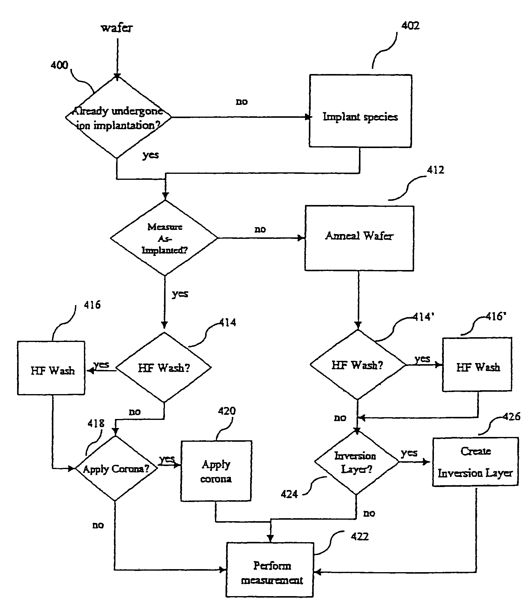
[0034]Embodiments of the present invention will be more completely understood through the following detailed description, which should be read in conjunction with the attached drawings. In this description, like numbers refer to similar elements within various embodiments of the present invention. Within this detailed description, the claimed invention will be explained with respect to embodiments. However, the skilled artisan will readily appreciate that the embodiments described herein are merely exemplary and that variations can be made without departing from the spirit and scope of the invention.

[0035]Given the high costs associated with semiconductor processing, techniques and devices that help eliminate defective wafers before and during wafer processing are of great value. Specifically, the ability to detect defects non-destructively via electrical characterization of wafers is valuable because such an approach is easily integrated into existing fabrication systems.

[0036]The ...


PUM


Abstract

The invention relates to the use of the metrology methods and the related apparatus disclosed herein that incorporate thermal treatment devices and methods that improve defect detection. Specifically, in one aspect the invention relates to method of thermally treating a semiconductor wafer such that an acceleration of interstitial defect migration is achieved while leaving vacancy defects substantially unaltered.

Description

RELATED APPLICATION[0001]This application claims priority to U.S. Provisional Application 60 / 661,557 filed on Mar. 14, 2005, the disclosure of which is herein incorporated by reference in its entirety.FIELD OF THE INVENTION[0002]The invention relates to the testing of semiconductor wafers during manufacturing and specifically to the real-time in-line testing of semiconductor wafers during integrated circuit-fabrication.BACKGROUND OF THE INVENTION[0003]There are numerous individual operations, or processing steps, performed, in a strictly followed sequence, on a silicon wafer in the course of manufacturing a complex integrated circuit (IC). Each such operation must be precisely controlled in order to assure that the entire fabrication process yields integrated circuits displaying the required electrical characteristics.[0004]Frequently, failure of an individual operation is detected only after the completion of the entire, very expensive, process of IC fabrication. Due to the very hi...

Claims


Application Information

Patent Timeline
Patent Type & Authority Patents(United States)
IPC IPC(8): G01R31/302
CPCG01R31/311H01L22/14H01L22/20G01R31/2648H01L2924/0002H01L2924/00
Inventor STEEPLES, KENNETHTSIDILKOVSKI, EDWARD
Owner SEMILAB SEMICON PHYSICS LAB
Why Eureka
Try Eureka