Method for generating a set of test patterns for an optical proximity correction algorithm

a technology of optical proximity correction and pattern generation, applied in the field of vlsi design, can solve the problems of failure or production of layouts faulty for inputted patterns, deviation of normal patterns produced on the wafer, and inability to accurately cover the layou

Inactive Publication Date: 2008-07-22
GLOBALFOUNDRIES INC
View PDF1 Cites 11 Cited by
  • Summary
  • Abstract
  • Description
  • Claims
  • Application Information

AI Technical Summary

Problems solved by technology

However, the patterns produced on the wafer normally differ from those designed due to pattern dependent optical distortions when exposure wavelengths are greater than the feature line width.
However, while such OPC algorithms may work for most layouts, they may fail or produce faulty layouts for certain inputted patterns.
One problem that arises then is how to create an optimal set of patterns for this testing.
In both approaches, however, it is unknown how effectively the layout covers the space of possible shape interactions that may reveal flaws in the OPC algorithm.

Method used


Image

  • Method for generating a set of test patterns for an optical proximity correction algorithm
  • Method for generating a set of test patterns for an optical proximity correction algorithm
  • Method for generating a set of test patterns for an optical proximity correction algorithm

Examples


Embodiment Construction

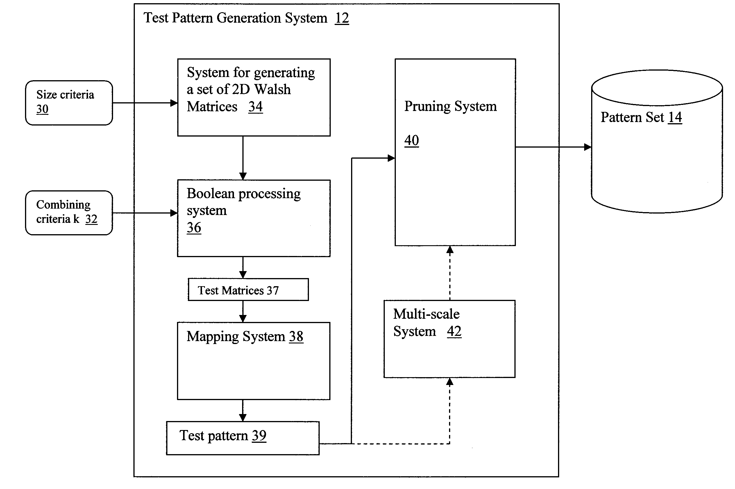
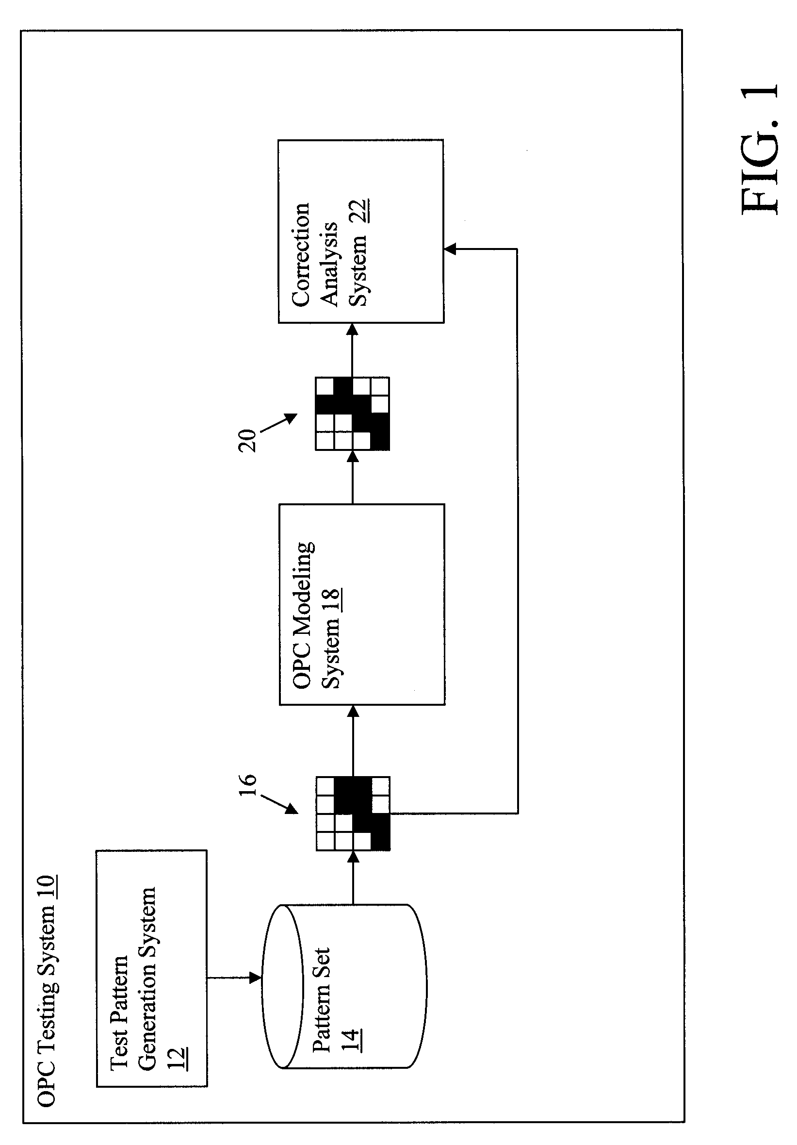
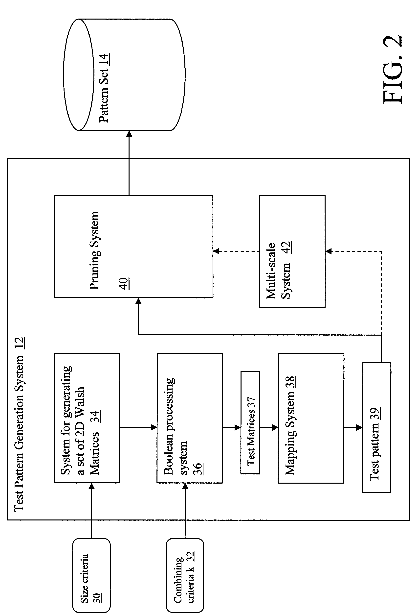
[0018]Referring now FIG. 1, an illustrative optical proximity correction (OPC) testing system 10 is shown. OPC testing system 10 includes a test pattern generation system 12 that generates a pattern set 14 that will be used to test an OPC algorithm. To accomplish this testing, individual patterns 16 are inputted to an OPC modeling system 18 to generate a modeled output 20. Modeled output 20 describes, e.g., how the inputted pattern 16 would translate onto a wafer using a particular OPC algorithm. A correction analysis system 22 can analyze the modeled output 20 to determine if the OPC algorithm will generate a faulty result for the inputted pattern. Thus, OPC modeling system 18 and correction analysis system 22 form a correction process that verifies topological equivalence, e.g., ensuring that no shorts (reduced number of shapes) or opens (increased number of shapes) are created. It should be understood that the OPC testing system 10 shown in FIG. 1 is provided for illustrative pur...


PUM


Abstract

A method of synthesizing layout patterns to test an optical proximity correction algorithm. The method comprises the steps of: embodying Walsh patterns in a set of Walsh pattern matrices; processing groups of matrices from the set of Walsh pattern matrices to form a set of test matrices; mapping the set of test matrices to a test pattern set.

Description

BACKGROUND OF INVENTION[0001]1. Technical Field[0002]The present invention relates generally to VLSI design, and more particularly relates to a system and method for testing optical proximity correction algorithms for VLSI design.[0003]2. Related Art[0004]Optical lithography for very large scale integrated (VLSI) circuits is implemented by exposing resist on wafers in a pattern defined by designed shapes on a mask. However, the patterns produced on the wafer normally differ from those designed due to pattern dependent optical distortions when exposure wavelengths are greater than the feature line width. A variety of resolution enhancement techniques, including optical proximity correction (OPC) algorithms, have been devised to compensate for this effect. These OPC algorithms modify the designed layouts in ways so that the actual wafer layout more closely matches the original ideal layout. However, while such OPC algorithms may work for most layouts, they may fail or produce faulty l...

Claims


Application Information

Patent Timeline
Patent Type & Authority Patents(United States)
IPC IPC(8): G06F17/50
CPCG06F17/5081G06F2217/12G06F2119/18G06F30/398Y02P90/02
Inventor DEMARIS, DAVID L.LAVIN, MARK A.LEIPOLD, WILLIAM C.MAYNARD, DANIEL N.MUKHERJEE, MAHARAJ
Owner GLOBALFOUNDRIES INC
Why Eureka
Try Eureka