Light-emitting device, display device, and stress sensor

a display device and light-emitting device technology, applied in the direction of discharge tube luminescnet screen, discharge tube/lamp details, force measurement by measuring optical property variation, etc., to achieve the effect of simple structure, long lasting and easy production

Inactive Publication Date: 2008-08-05
NAT INST OF ADVANCED IND SCI & TECH
View PDF9 Cites 9 Cited by
  • Summary
  • Abstract
  • Description
  • Claims
  • Application Information

AI Technical Summary

Benefits of technology

[0017]The present invention was made in view of the foregoing conventional problems, and an object of the present invention is to provide a light-emitting device which is pollution-free, longer lasting, easy to produce, simple in structure, and strong. Moreover, another object of the present invention is to provide a display device which has a high image quality, high crashworthy and high heat resistance, and is pollution-free. Furthermore, a further object of the present invention is to provide a stress sensor which can easily measure a stress distribution state of measuring object.
[0020]Moreover, the electric inductive distortion material and the stress light-emitting material can be formed without using materials, which cause environmental problems, such as mercury which is used in a conventional fluorescent lamp. As such, the electric inductive distortion material and the stress light-emitting material will never cause any environmental problems. Moreover, the light-emitting device of the present invention has a two-section structure of the electrostriction section and the stress light-emitting section. Therefore, as compared with a conventional fluorescent character display tube, the light-emitting device of the present invention has a simpler and stronger structure, and is easily manufactured.
[0021]Furthermore, unlike the conventional incandescent lamp which emits the light based on the heat emission, the light-emitting device of the present invention emits the light by utilizing the nature in which the electrons excited by the mechanical energy carries out luminescence when the electrons thus excited move back toward the ground state. As such, the light-emitting device does not bring about the heat rise caused by the light emission. That is, the light-emitting device of the present invention can last long, have good luminous efficiency, and is compact and strong.
[0022]Therefore, it is possible to provide the light-emitting device, which is pollution-free, long-lasting, easy to produce, simple in structure, and strong.

Problems solved by technology

Moreover, the electric inductive distortion material and the stress light-emitting material can be formed without using materials, which cause environmental problems, such as mercury which is used in a conventional fluorescent lamp.

Method used


Image

  • Light-emitting device, display device, and stress sensor
  • Light-emitting device, display device, and stress sensor
  • Light-emitting device, display device, and stress sensor

Examples


example

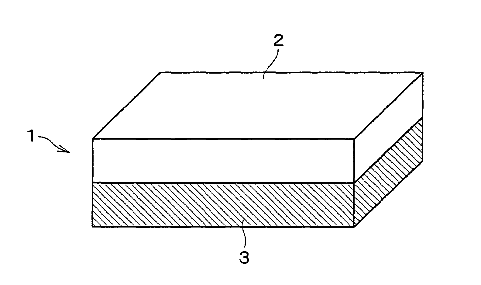
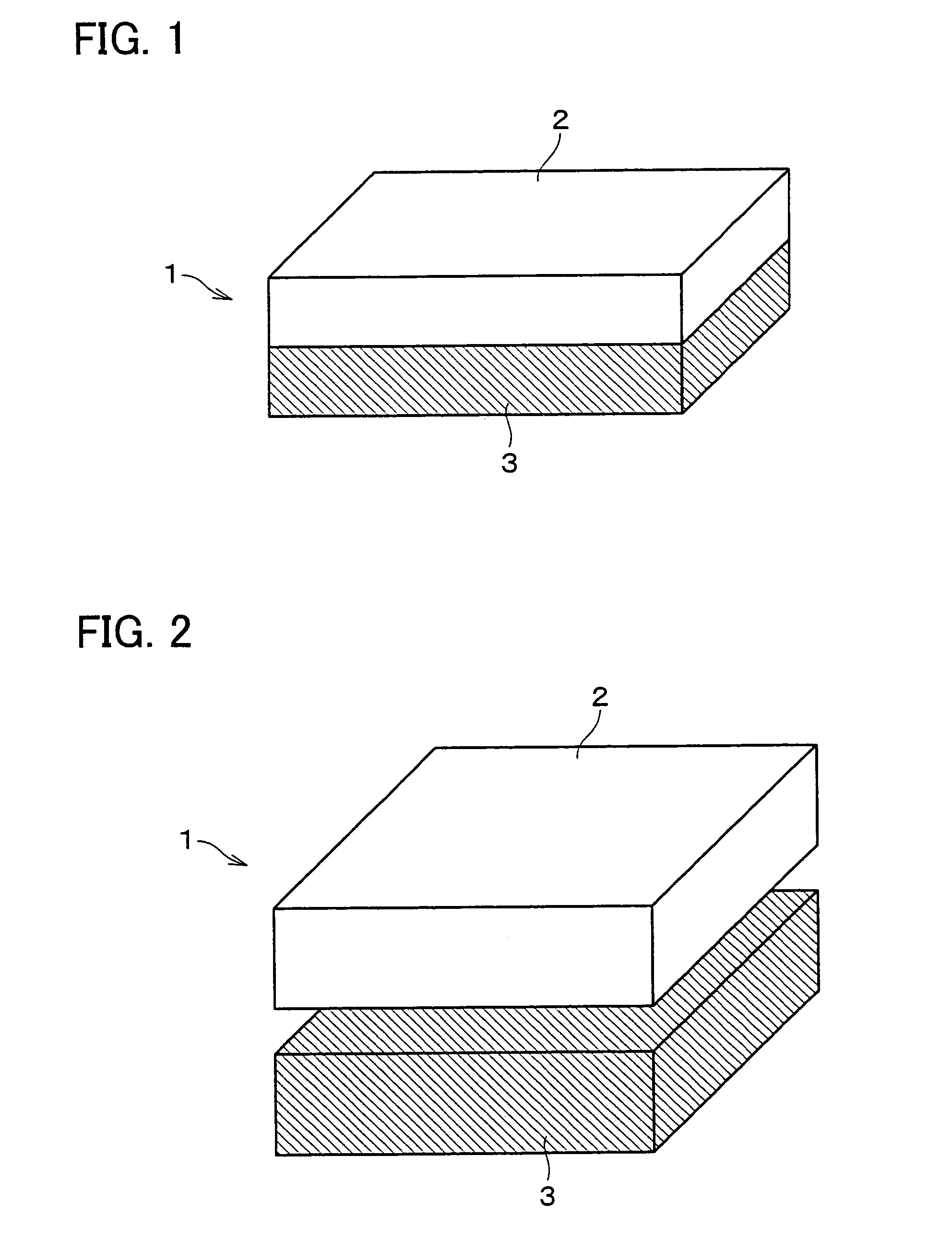
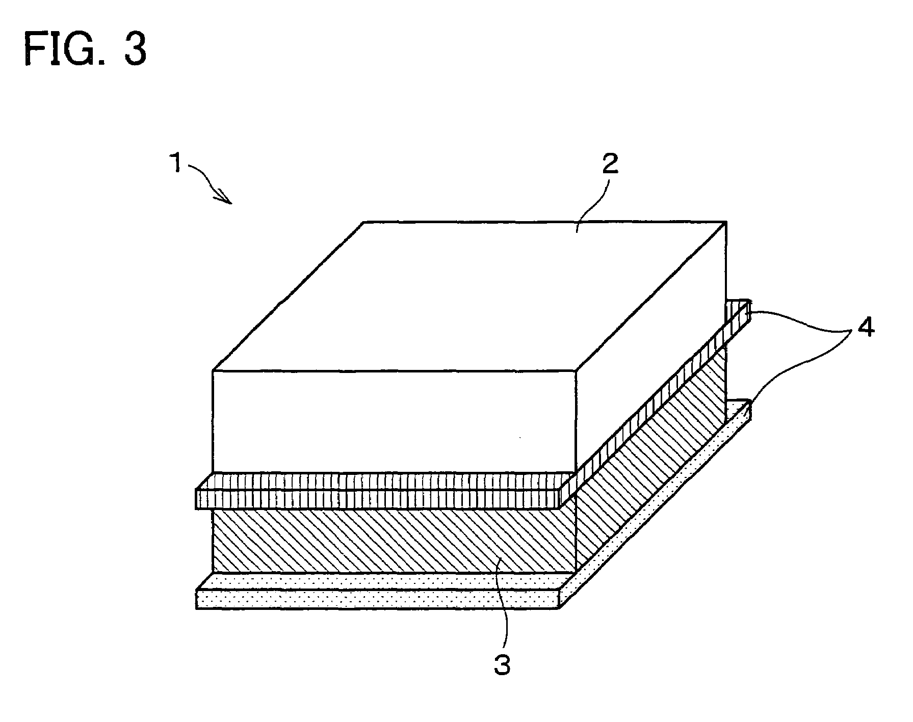
[0087]The following description deals with a verified characteristic of the luminescence intensity of the stacked structure 1 in accordance with the First Embodiment of the present invention. Here, PMN (PbMgNbO3), which is aligned by the sputtering, is used as the electric inductive distortion material in the electrostriction layer 2, and strontium aluminate is used as the stress light-emitting material in the stress light-emitting layer 3.

[0088]FIG. 6 is a graph showing a relationship, in the stacked structure 1 of the above structure, between the stress applied to the stress light-emitting layer 3 and the luminous intensity. As shown in FIG. 6, it was clear that the luminous intensity depended on the stress, and that the luminescence intensity increased with an increase in the stress.

[0089]Moreover, FIG. 7 is a graph showing a relationship between a strain ratio of the electrostriction layer 2 and the luminous intensity. As shown in FIG. 7, it was clear that the luminous intensity...


PUM

PropertyMeasurementUnit
thicknessaaaaaaaaaa
thicknessaaaaaaaaaa
thicknessaaaaaaaaaa

Abstract

A stacked structure (1) includes an electrostriction layer (2) including an electric inductive distortion material and a stress light-emitting layer (3) including a stress light-emitting material. When applying a voltage to the electrostriction layer (2) in the stacked structure (1), the electric inductive distortion material deforms, thereby the electrostriction layer (2) deforms. The deformation of the electrostriction layer (2) causes an external force to act on the stress light-emitting material of the stress light-emitting layer (3), and the stress light-emitting layer (3) emits light, accordingly. That is, by applying the voltage to the stacked structure (1), the stacked structure (1) can emit the light.

Description

[0001]This application is a 371 of PCT international application Ser. No. PCT / JP03 / 03230, filed on Mar. 18, 2003.TECHNICAL FIELD[0002]The present invention relates to a novel light-emitting device, a display device, and a stress sensor, which emit light in response to a deformation due to an externally applied voltage.BACKGROUND ART[0003]Conventionally used as a typical light-emitting device are a light emitting diode (LED), a vacuum fluorescent display (VFD), a fluorescent lamp, an incandescent lamp, or the like.[0004]In a field of a display using LED (serving as the light-emitting device), an LED which emits blue light has been developed. Since red, green, and blue LEDs have been lined up, it is possible to carry out a full-color display. Thousands of three-color LEDs are provided in most of existing supersized full-color screens.[0005]In addition, used as another existing displays are a CRT (Cathode-Ray Tube) display, a plasma display, a liquid crystal display, or the like.[0006]...

Claims


Application Information

Patent Timeline
Patent Type & Authority Patents(United States)
IPC IPC(8): H05B33/00H05B33/22G01L1/24H01L41/08
CPCH01L41/08G01L1/24H10N30/00
Inventor XU, CHAO-NANTATEYAMA, HIROSHI
Owner NAT INST OF ADVANCED IND SCI & TECH
Why Eureka
Try Eureka