
Total configuration memory cell validation built in self test (BIST) circuit

a self-testing, total configuration technology, applied in the direction of instruments, computation using denominational number representation, pulse technique, etc., can solve the problems of reducing the mean time to failure resulting from seus, more prone to errors in configuration memory, and increasing the probability of collisions between on-chip memory cells and cosmic particles

Active Publication Date: 2008-08-05
XILINX INC
View PDF4 Cites 40 Cited by
  • Summary
  • Abstract
  • Description
  • Claims
  • Application Information

AI Technical Summary

Benefits of technology

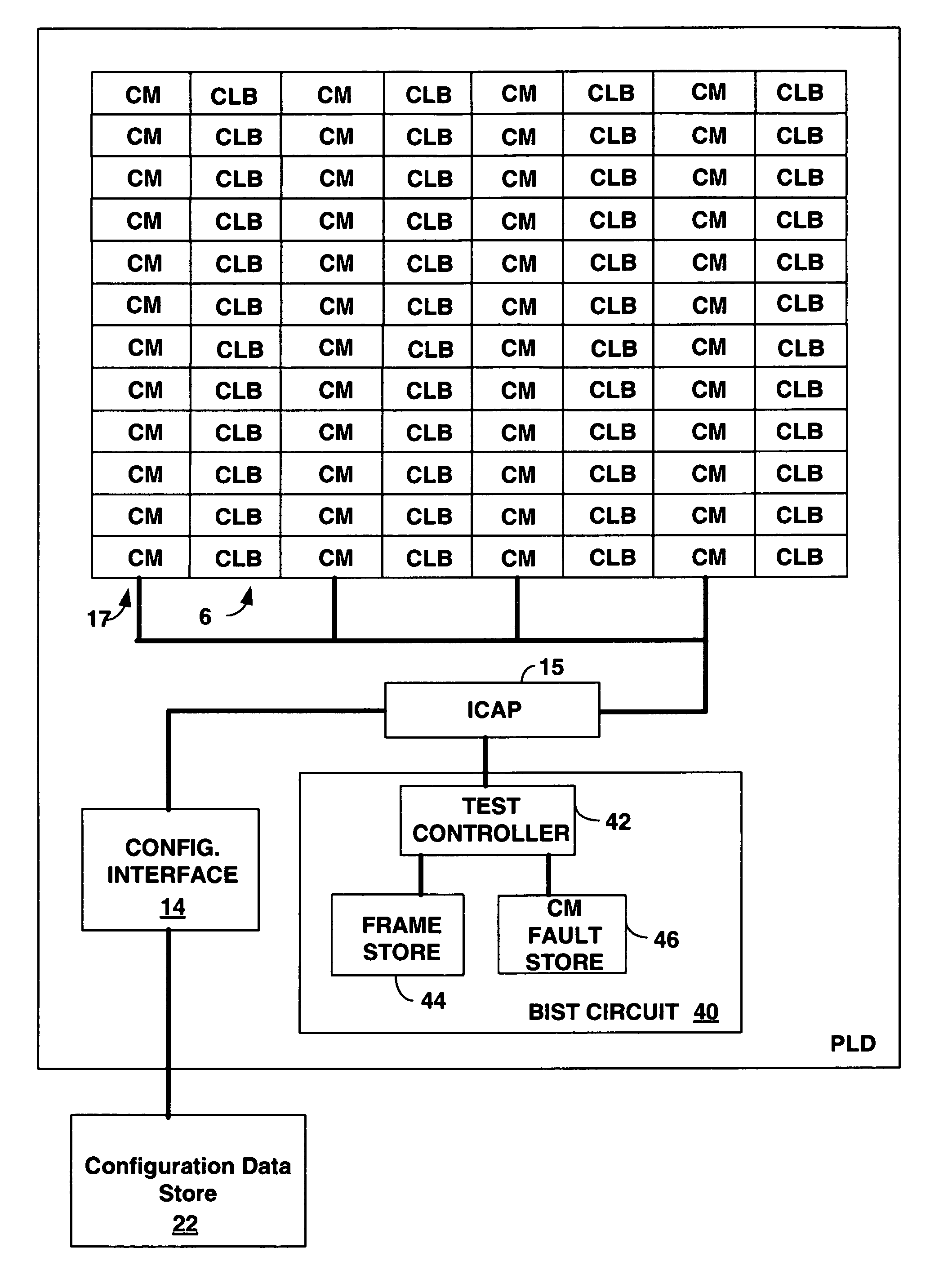
[0012]Embodiments of the present invention provide BIST circuitry for validating 100% of the configuration memory cells for “stuck-at” faults resulting from defects in individual configuration memory cells. The BIST circuitry further uses the ICAP to write to and read from the configuration memory cells frame by frame to enable detection of SEUs with minimal circuitry. Further, the BIST circuit enables efficient writing and read back of recurring bit patterns at power up in a production environment without knowledge of how the PLD will later be configured.
[0013]The BIST for embodiments of the present invention is constructed from fixed logic or hard core logic including circuitry to use the ICAP to write individual frames and read back the written data to enable the validation of every configuration bit. A small memory is included with the BIST circuit for storing the frame being evaluated. Testing is performed by writing and then reading back bit recurring patterns in a frame, comparing bits to the expected written pattern, noting the differences. The recurring patterns can include checkerboards, walking 1's all 0 / 1's etc. These bit flip patterns enable testing the configuration memory without the need to functionally configure the PLD. Testing can, thus, be performed in a production environment without knowledge of how the PLD will be configured.

Problems solved by technology

With higher densities of configuration memory cells on PLDs, the configuration memory, however, is more prone to errors.
As transistor geometries become smaller and supply voltages become lower, on-chip memory cells are becoming more likely to be upset by collisions with cosmic particles, or single event upsets (SEUs).
Having a greater number of configuration memory cells on a chip decreases the mean time to failure resulting from SEUs.
As PLD configuration memory density increases, it is further increasingly difficult to test for memory faults, or to account for the effect of SEUs.
This testing is time-consuming and typically requires significant testing software provided external to the PLD.

Method used


Image

  • Total configuration memory cell validation built in self test (BIST) circuit
  • Total configuration memory cell validation built in self test (BIST) circuit
  • Total configuration memory cell validation built in self test (BIST) circuit

Examples


Embodiment Construction

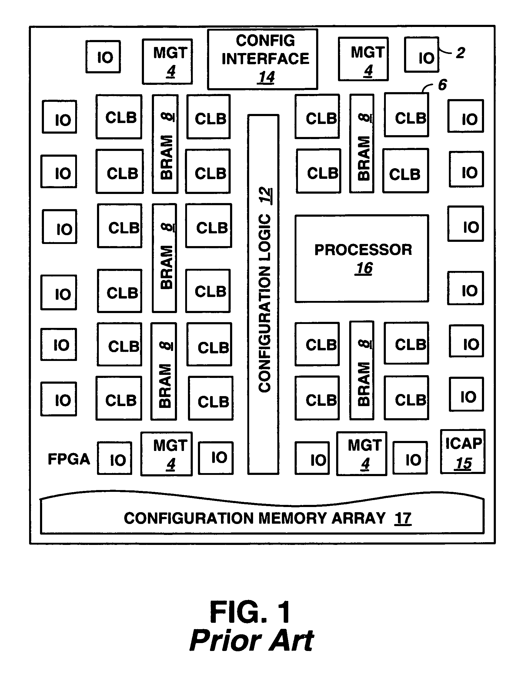
[0021]Embodiments of the present invention provide for testing the configuration memory for faults by taking advantage of partial configuration. The Virtex-4 FPGA manufactured by Xilinx, Inc. of San Jose, Calif., includes an ICAP providing for partial configuration on a frame by frame basis. Efficient partial reconfiguration of an FPGA is performed by only reading and rewriting a portion of the frames or columns in the configuration memory array at a time. Efficient operation can result using partial reconfiguration for a BIST circuit because storage of only a frame of the configuration memory is required at one time.

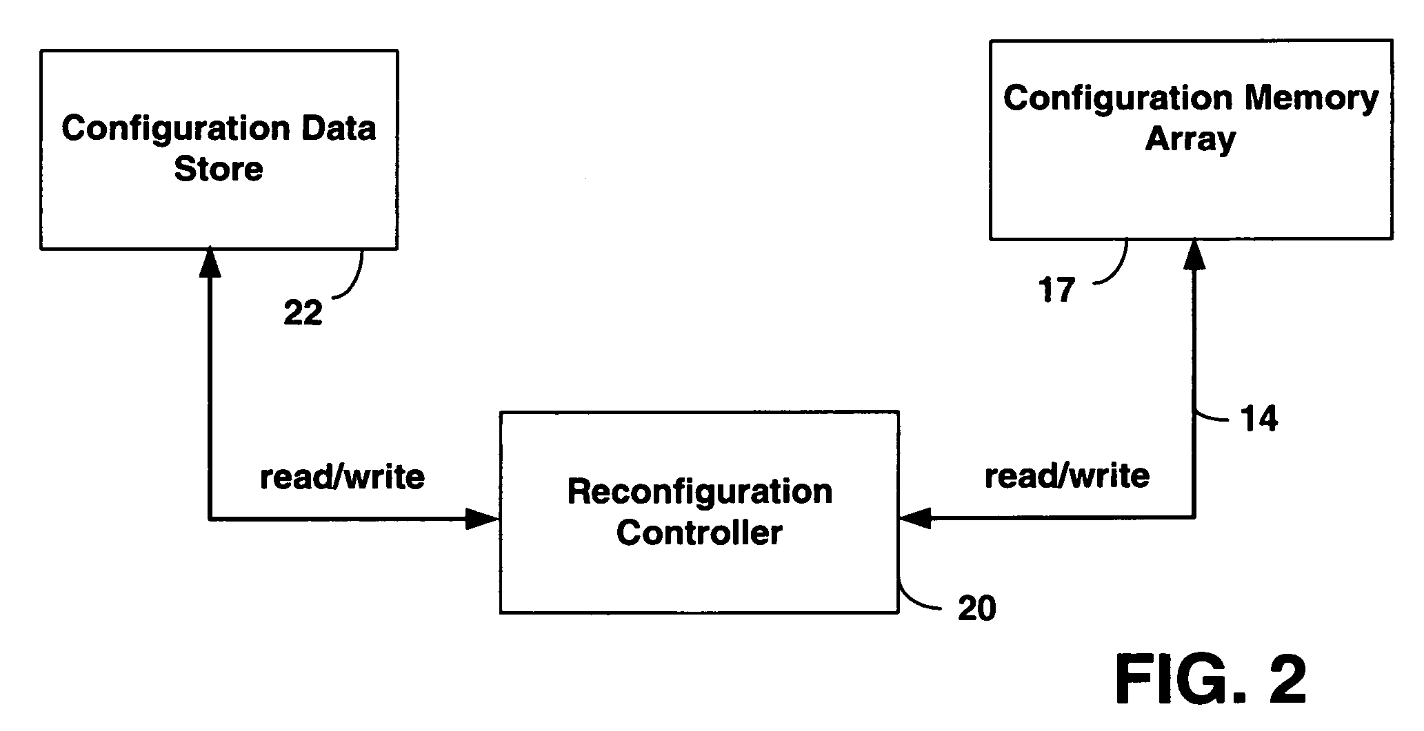
[0022]FIG. 2 shows one configuration of circuitry used to enable efficient partial reconfiguration using an ICAP, such as in the Virtex-4 FPGA. To control reading and writing of data into the configuration memory array 17, a controller 20 is used. The controller 20 can be included with the ICAP 15 internal to the FPGA. Alternatively, the controller 20 may be a separate ...


PUM


Abstract

A built in self test (BIST) circuit is provided for a programmable logic device (PLD) constructed from fixed or hard core logic that includes circuitry to write recurring patterns of bits in the configuration memory in a frame by frame manner and read the cell state to enable the validation of every configuration bit at power up. The BIST circuitry can further be used to program the recurring patterns into the configuration memory, and then read frames of the configuration memory to detect the occurrence of single event upsets (SEU) that corrupt data in the configuration memory. The recurring patterns programmed do not require time consuming functional configuration of the PLD, and can be done in a production environment after power up without knowledge of how the PLD will later be configured. No soft logic is needed to form the BIST circuit, enabling 100% test coverage of the programmable configuration memory cells.

Description

BACKGROUND[0001]1. Technical Field[0002]The present invention relates to a built in self test system for a Programmable Logic Device (PLD). More particularly, the present invention relates to a BIST that detects faulty configuration memory cells and provides for debugging of various programming scenarios for configuration memory cells.[0003]2. Related Art[0004]Traditional PLDs such as Field Programmable Gate Arrays (FPGAs) and Complex PLDs (CPLDs) typically use millions of Static Random Access Memory (SRAM) cells forming a configuration memory to program the functionality of the implemented circuit. This programmability leads to many advantages such as ease of use, fast time-to-market, low non-recurrent engineering expenses, and on-chip design verification. With higher densities of configuration memory cells on PLDs, the configuration memory, however, is more prone to errors.[0005]As transistor geometries become smaller and supply voltages become lower, on-chip memory cells are beco...

Claims


Application Information

Patent Timeline
Patent Type & Authority Patents(United States)
IPC IPC(8): G01R31/28G06F7/38G11C29/00
CPCG01R31/318544G01R31/3187G11C29/44G11C29/48G11C29/34G11C11/41G11C2029/0407G11C2029/0401
Inventor DRIMER, SAAR
Owner XILINX INC
Learn More