Resist pattern-improving material and a method for preparing a resist pattern by using the same

a technology of resist pattern and improving material, which is applied in the field of resist pattern improvement material and a method for preparing a pattern, can solve the problems of significant affecting the yield of the product, unavoidable edge roughness, and pattern accompanied with edge roughness is not precisely appropriate for the pattern, so as to improve the resist material and reduce the edge roughness. , the effect of improving the resist material

Inactive Publication Date: 2008-08-26
FUJITSU LTD
View PDF28 Cites 11 Cited by
  • Summary
  • Abstract
  • Description
  • Claims
  • Application Information

AI Technical Summary

Benefits of technology

[0009]Therefore, there is an objective to be solved in this invention. That is a reduction of an edge roughness during forming a fine pattern, which was difficult to avoid only by improving a resist material. Such an objective is solved by that after patterning a resist film, a coating film is formed on the resist film, so as to intermix the resist film material with the coating film material at the interface therebetween to reduce the edge roughness. In addition to reducing the edge roughness, there is also an objective to keep or improve etching resistance, not only by using a resist material which is used for irradiation by means of a light source having a wavelength in the field of a deep ultraviolet, such as, an ArF (argon fluoride) excimer laser, but also by using a resist material which is used for irradiation by means of a light source, such as, KrF (krypton fluoride) excimer laser, and which is known to have superior etching resistance.

Problems solved by technology

However, when using a far ultraviolet ray having a shorter wavelength than ever as an irradiating light, edge roughness is unavoidable: that is, the smaller or finer the resist pattern is designed, the more the edge of the resist pattern is waved, although the edge is designed to be formed in a line shape.
As a result, the edge roughness will significantly affect the yield of the product.
However, such a resist pattern accompanied with the edge roughness is not appropriate for precisely etching the conductive film and patterning by remaining the portion of the slashed portions as shown.
However, if a pattern is formed by being transferred by the resist pattern having the edge roughness, it will be difficult to cover a copper diffusion prevention film of such a copper wiring, resulting in significantly affecting the following steps after the lithography step or resulting in loss of reliability of the device.
These improvements may compromise the reduction of the edge roughness.
Therefore, it has been more difficult to reduce the edge roughness while improving the other properties.
As a result, the edge roughness will more affect the quality of the devices than ever, especially at the step after forming the resist pattern, such as, an etching step or wiring step, resulting in causing short circuit of the wiring or disconnection of the pattern.

Method used


Image

  • Resist pattern-improving material and a method for preparing a resist pattern by using the same
  • Resist pattern-improving material and a method for preparing a resist pattern by using the same
  • Resist pattern-improving material and a method for preparing a resist pattern by using the same

Examples


Embodiment Construction

[0087]The technology of the resist pattern-improving material according to the present invention may be useful for various applications, among which several methods for preparing various devices are explained here.

(1) First Application Example of the Present Invention: A Method for Preparing a Flash Memory

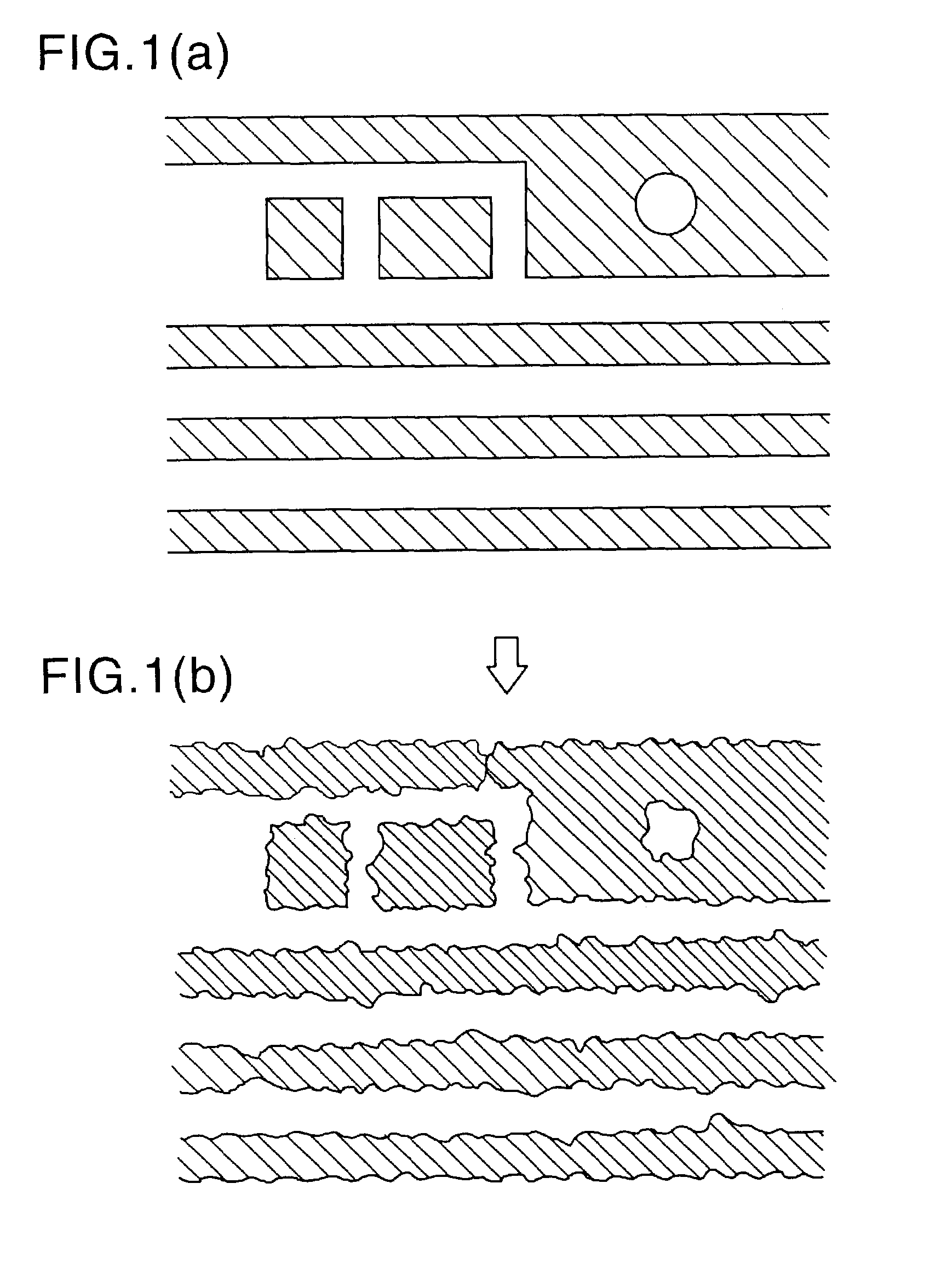
[0088]There is provided a method for preparing a flash memory. This is an example for preparing a semiconductor device, which may be preferable to incorporate the step for forming a pattern according to the present invention. For example, the resist pattern-improving material according to the present invention may be used in the step of forming a holed pattern, which may contribute to reduce an edge roughness of the resist pattern, and thereby, the size of the inner diameter of the holed pattern, the width between the linier patterns and / or separated patterns, and the interval between the linear patterns, and so on, may be controlled within the allowable range

[0089]As shown in FIG....


PUM

PropertyMeasurementUnit
sizeaaaaaaaaaa
thicknessaaaaaaaaaa
boiling pointaaaaaaaaaa

Abstract

The present invention provided an improvement to reduce an edge roughness during forming a small and fine pattern. Such and objective is to accomplish that after patterning a resist film, a coating film is formed on the resist film, so as to intermix the resist film material with the coating film material at the interface therebetween to reduce the edge roughness. There is provided a resist pattern-improving material, comprising: (a) a water-soluble or alkali-soluble composition, comprising: (i) a resin, and (ii) a crosslinking agent. Alternatively, The resist pattern-improving material, comprising (a) a water-soluble or alkali-soluble composition, comprising: (i) a resin, and (ii) a nonionic surfactant. According to the present invention, a pattern is prepared in the step, comprising: (a) forming a resist pattern; and (b) coating the resist pattern-improving material on the surface of the resist pattern. According to the present invention, the resist pattern-improving material is mixed with the resist pattern at the interface therebetween. The resist pattern may be formed by irradiating a ArF excimar laser light or a laser light having a wavelength shorter than that of the ArF excimar laser light. The pattern of the resist pattern-improving material includes a base resin which does not substantially transmit the ArF excimar laser light.

Description

CROSS-REFERENCE TO RELATED APPLICATION[0001]This application is based upon and claims the benefit of priority from the prior Japanese Patent Application No. 2002-59429, filed on Mar. 5, 2002, the entire contents of which are incorporated herein by reference.FIELD OF THE INVENTION[0002]The present invention relates to a resist pattern-improving material and a method for preparing a pattern by using the same. The present invention, in particular, relates to an improvement for forming a coating layer on the surface of the resist pattern by photo irradiation, and intermixing the coating layer with the surface of the resist pattern, and thereby reducing an edge roughness of the pattern. Such a pattern is used in semiconductor devices, magnetic sensors, various functional parts, and so on.RELATED ART[0003]Photo irradiation techniques are generally efficient for mass production. In order to continue to improve the efficiency of mass productivity, there has been a demand to use the photo ir...

Claims


Application Information

Patent Timeline
Patent Type & Authority Patents(United States)
IPC IPC(8): G03C5/00G03F7/00G03F7/40H01L21/027
CPCG03F7/0035G03F7/40H01L21/0275Y02E50/30Y02W30/40H01L21/027
Inventor NOZAKI, KOJIKOZAWA, MIWA
Owner FUJITSU LTD
Why Eureka
Try Eureka