Method for forming a metallization layer stack to reduce the roughness of metal lines

a technology of metallization layer and metallization layer stack, which is applied in the manufacturing of basic electric elements, electrical equipment, semiconductor/solid-state devices, etc., can solve the problems of reducing line reliability, increasing leakage current, and changing one process or material that may typically require great effort, so as to reduce the deleterious effect, reduce the dimension, and reduce the edge roughness of the trench significantly.

Active Publication Date: 2007-10-09
ADVANCED MICRO DEVICES INC
View PDF8 Cites 2 Cited by
  • Summary
  • Abstract
  • Description
  • Claims
  • Application Information

AI Technical Summary

Benefits of technology

[0016]Generally, the present invention is directed to a technique that enables the reduction of deleterious effects of an anisotropic etch process, even if a moderately thin resist mask is used. For this purpose, a low-k dielectric layer stack may be provided so that, in combination with an appropriately designed etch recipe, trenches with reduced dimensions may be formed, wherein the edge roughness of the trench is significantly reduced compared to the conventional approach.

Problems solved by technology

Since the plurality of process steps involved in finally obtaining a circuit element of specified dimensions mutually influence each other, the change of one process or material may typically require great effort in establishing a new appropriate process sequence that conforms with the new design and process requirements.
As previously noted, since the thickness 110a of the resist mask 110 may not be increased arbitrarily to substantially reduce the erosion of the edge regions 113, especially during the final etch step for opening the etch stop layer 105, owing to lithographical constraints, a high roughness at the trench edge is obtained, which may finally lead to increased leakage current and reduced line reliability, after coating the trench 112 with a barrier material and filling it with a metal, such as copper.

Method used


Image

  • Method for forming a metallization layer stack to reduce the roughness of metal lines
  • Method for forming a metallization layer stack to reduce the roughness of metal lines
  • Method for forming a metallization layer stack to reduce the roughness of metal lines

Examples


Embodiment Construction

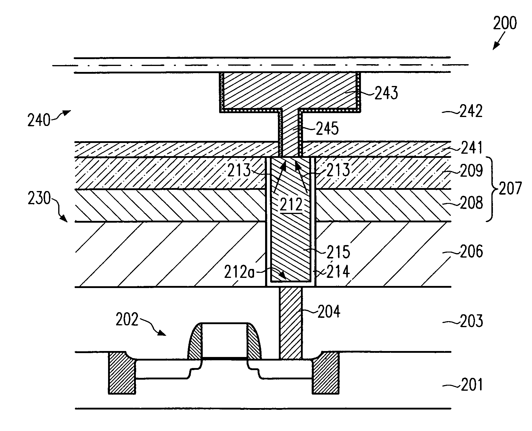
[0026]Illustrative embodiments of the invention are described below. In the interest of clarity, not all features of an actual implementation are described in this specification. It will of course be appreciated that in the development of any such actual embodiment, numerous implementation-specific decisions must be made to achieve the developers specific goals, such as compliance with system-related and business-related constraints, which will vary from one implementation to another. Moreover, it will be appreciated that such a development effort might be complex and time-consuming, but would nevertheless be a routine undertaking for those of ordinary skill in the art having the benefit of this disclosure.

[0027]The present invention will now be described with reference to the attached figures. Although the various regions and structures of a semiconductor device are depicted in the drawings as having very precise, sharp configurations and profiles, those skilled in the art recogniz...


PUM


Abstract

A method for making a simplified dielectric layer stack for the first metallization layer is provided in combination with an improved anisotropic etch process, wherein the etch attack at the trench perimeter is reduced for a patterning process on the basis of a 193 nm lithography. In the simplified layer stack, a bottom etch stop layer formed beneath a low-k dielectric layer may be omitted, thereby reducing production costs while enhancing product performance by lowering leakage currents in the first metallization layer.

Description

BACKGROUND OF THE INVENTION[0001]1. Field of the Invention[0002]The present invention generally relates to the fabrication of integrated circuits, and, more particularly, to the formation of metal lines formed in a low-k dielectric material, wherein the dimensions of the metal line trenches may be defined by a 193-nm lithography technique.[0003]2. Description of the Related Art[0004]The fabrication of an integrated circuit is a highly complex process requiring up to 500 or even more single process steps for sophisticated semiconductor devices, such as microprocessors, storage devices, ASICs (application specific integrated circuits) and the like, wherein one of the most critical process steps is the lithographical imaging of a specified circuit pattern provided on a mask or reticle into a resist layer formed on a substrate and the subsequent patterning of the resist layer. The patterned resist layer is then used as a mask for the subsequent patterning of underlying material layers b...

Claims


Application Information

Patent Timeline
Patent Type & Authority Patents(United States)
IPC IPC(8): H01L21/4763H01L21/283H01L21/311H01L21/44H01L21/768
CPCH01L21/31116H01L21/76802H01L21/31144H01L21/76804
Inventor FROHBERG, KAISCHALLER, MATTHIAS
Owner ADVANCED MICRO DEVICES INC
Why Eureka
Try Eureka