Method of manufacture of ceramic composite wiring structures for semiconductor devices

a technology of ceramic composite wiring and semiconductor devices, applied in the field of ceramic composite circuit wiring boards and/or multi-chip modules, can solve the problems of reducing circuit performance, reducing the volume fraction of solid state ceramic, and limiting the physical dimensions of si

Inactive Publication Date: 2006-05-23
L PIERRE DEROCHEMONT C2 TECH
View PDF88 Cites 74 Cited by
  • Summary
  • Abstract
  • Description
  • Claims
  • Application Information

AI Technical Summary

Benefits of technology

[0024]The volume fraction of solid state ceramic is less than the volume solution precursor as the decomposition (or unwanted reaction) products are removed. Thus, it is advantageous to utilize a high solid content precursor solution, which is often quite viscous; or to pyrolyze the precursor in situ as it is applied, as is the case when the precursors are spray pyrolyzed onto an already heated

Problems solved by technology

Conversely, this ultra-large scale integration restricts the physical dimensions of the SIC.
The drive to implement more sophisticated SIC's which require much larger numbers of electrical interconnections to be crammed into smaller physical dimensions creates a technical bottleneck, wherein SIC performance is increasingly limited by the circuit board/package connecting the chip to the larger electronic system.
This heat, if not dissipated from the SIC, reduces circuit performance.
Smaller lead sizes sharply limit their function as a heat

Method used


Image

  • Method of manufacture of ceramic composite wiring structures for semiconductor devices
  • Method of manufacture of ceramic composite wiring structures for semiconductor devices
  • Method of manufacture of ceramic composite wiring structures for semiconductor devices

Examples


Embodiment Construction

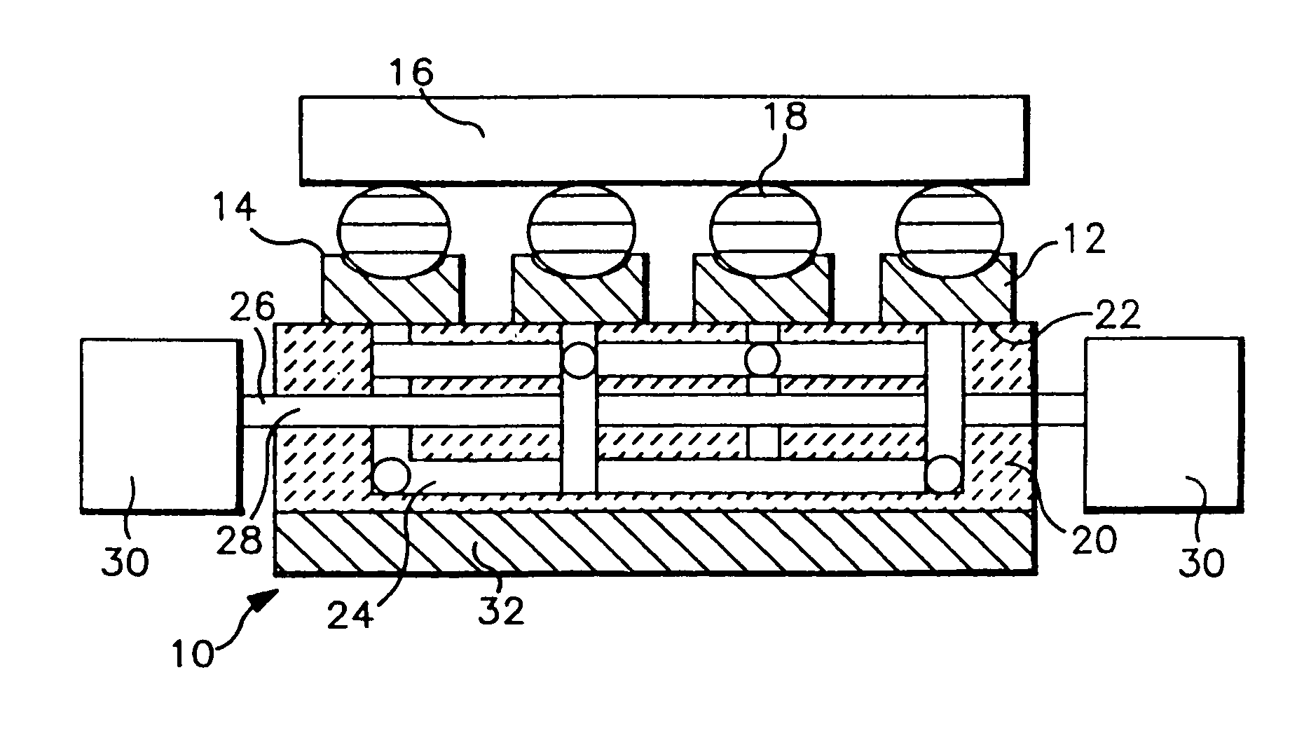
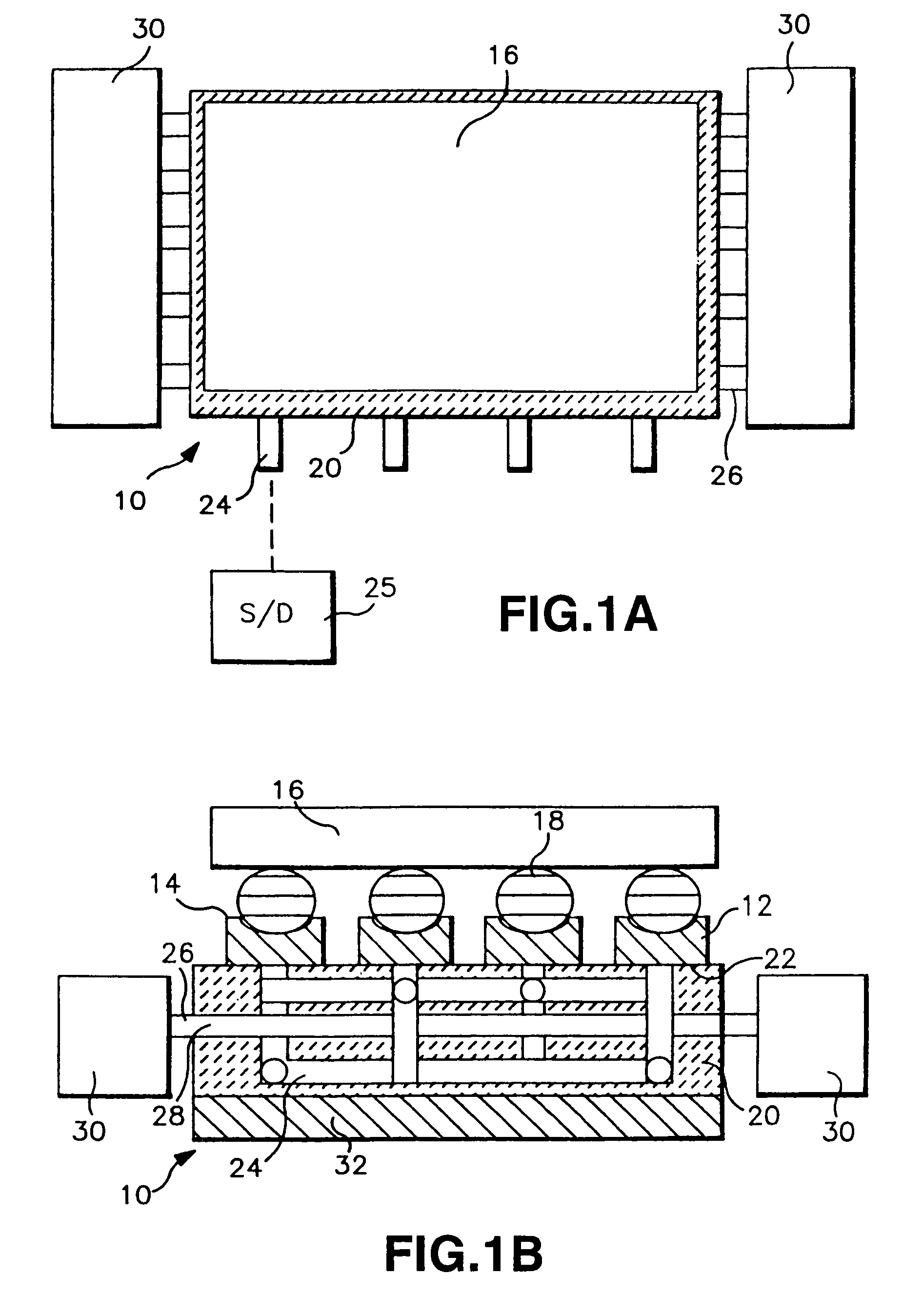
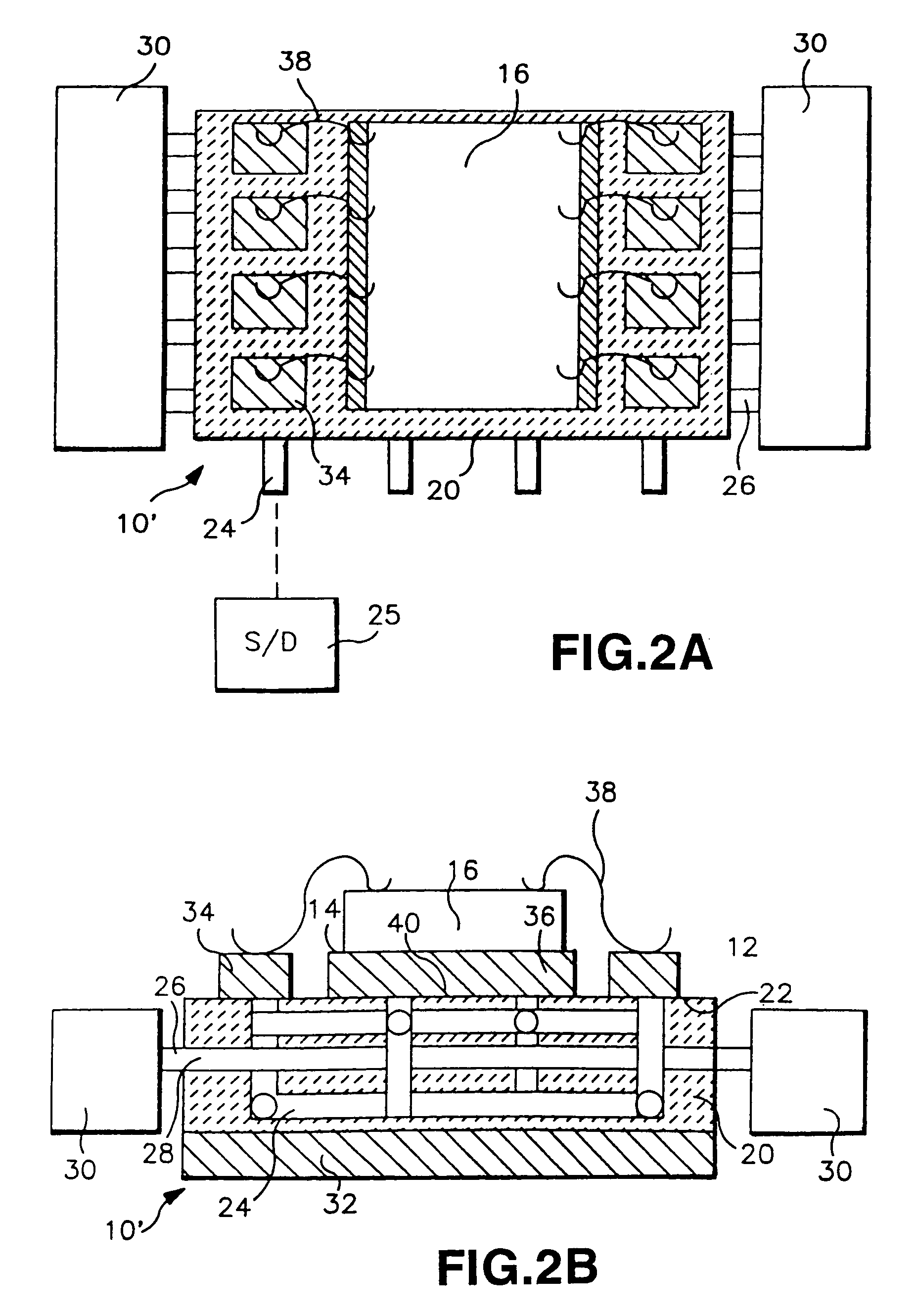
[0039]Reference is now made to FIGS. 1A, 1B, 2A and 2B which illustrate the preferred embodiments of the composite structure 10 and 10′ of this invention, also referred to as a composite wiring structure, while FIGS. 3A–3F illustrate the sequential steps used to create the composite structure with an electrical network, interconnects and heat sinks internal to the composite's dielectric member. For ease of understanding of this invention, like reference numerals will be used throughout the following description to identify identical elements illustrated in all embodiments.

[0040]The composite circuit wiring structure 10, although not limited thereto, is primarily used as a circuit wiring board, or, alternatively, as a multichip module. In the preferred embodiment of the invention shown in FIGS. 1A and 1B, the composite structure 10 has a top conductive, preferably metal member 12 with an exterior major surface 14 upon which at least one SIC 16 eventually will be mounted. Any suitable...


PUM

PropertyMeasurementUnit
Temperatureaaaaaaaaaa
Dielectric polarization enthalpyaaaaaaaaaa
Areaaaaaaaaaaa

Abstract

Method of manufacture of a composite wiring structure for use with at least one semiconductor device, the structure having a first conductive member upon which the semiconductor device can be mounted for electrical connection thereto. A dielectric member, made of ceramic or organo-ceramic composite material, is bonded to the first conductive member and contains embedded therein a conductive network and a thermal distribution network. A second conductive member may be incorporated with the composite wiring structure, with a capacitor electrically connected between the conductive network and the second conductive member. Bonding between the dielectric member and the conductive members may be in the form of a direct covalent bond formed at a temperature insufficient to adversely effect the structural integrity of the conductive network and the thermal distribution network.

Description

CROSS REFERENCE TO RELATED APPLICATIONS[0001]This Application is a divisional application of U.S. patent application Ser. No. 09 / 990,615, filed 21 Nov. 2001, now U.S. Pat. No. 6,742,249, and entitled “Method Of Manufacture Of Ceramic Composite Wiring Structures For Semiconductor Devices”, which is a divisional of U.S. patent application Ser. No. 09 / 344,682, now U.S. Pat. No. 6,323,549, filed 25 Jun. 1999 and entitled “Ceramic Composite Wiring Structures For Semiconductor Devices And Method Of Manufacture”, which is a continuation of International Application Serial No. PCT / US97 / 23976 filed 29 Dec. 1997, and a continuation-in-part of U.S. application Ser. No. 09 / 004,928 filed 09 Jan. 1998, now U.S. Pat. No. 6,143,432, which in turn is a continuation-in-part of U.S. patent application Ser. No. 08 / 697,739 filed 29 Aug. 1996 now U.S. Pat. No. 5,707,715. International Application Serial No. PCT / US97 / 23976 also claims priority of U.S. Provisional Application Ser. No. 60 / 033,983 filed 30 D...

Claims


Application Information

Patent Timeline
IPC IPC(8): H01R43/00H05K13/00B32B15/00H01L21/48H01L23/14H01L23/367H01L23/373H01L23/498H01L23/64H05K1/02H05K1/03H05K3/00H05K3/38
CPCB32B15/00H01L21/4857H01L23/142H01L23/3677H01L23/3735H01L23/49822H01L23/49833H01L23/642H05K1/0207H05K1/0271H05K3/202H05K3/38H05K3/46H01L21/4807Y10T29/4913H01L2221/68377H01L2224/16H01L2224/48472H01L2224/49175H01L2924/01039H01L2924/01057H01L2924/01077H01L2924/01079H01L2924/09701H01L2924/14H01L2924/19041H01L2924/3025H01L2924/3511H05K1/0272H05K1/0306H05K3/0061H05K3/4007H05K3/4629H05K3/4641H05K2201/0355H05K2201/09118H05K2203/0369H05K2203/1476H01L24/48H01L24/49Y10T29/49169Y10T29/49171Y10T29/49146Y10T428/24917H01L2224/45147Y10S428/901H01L2224/16225Y10T29/49128Y10T29/43H01L2924/00H01L2924/12042H01L24/45H01L2924/00014
Inventor DEROCHEMONT, L. PIERREFARMER, PETER H.
Owner L PIERRE DEROCHEMONT C2 TECH
Why Eureka
Try Eureka