Semiconductor structure and manufacturing method thereof

A manufacturing method and semiconductor technology, applied in semiconductor/solid-state device manufacturing, patterned surface photolithography, instruments, etc., can solve the problem of many defects, achieve less defects, reduce defects, reduce width uniformity and edge roughness degree of effect

Active Publication Date: 2019-05-03
INST OF MICROELECTRONICS CHINESE ACAD OF SCI
View PDF6 Cites 2 Cited by
  • Summary
  • Abstract
  • Description
  • Claims
  • Application Information

AI Technical Summary

Problems solved by technology

[0005] The main purpose of this application is to provide a semiconductor structure and its fabrication method to solve the problem of many defects in the semiconductor structure formed by the block copolymer directed self-assembly formation process in the prior art

Method used


Image

  • Semiconductor structure and manufacturing method thereof
  • Semiconductor structure and manufacturing method thereof
  • Semiconductor structure and manufacturing method thereof

Examples


Embodiment

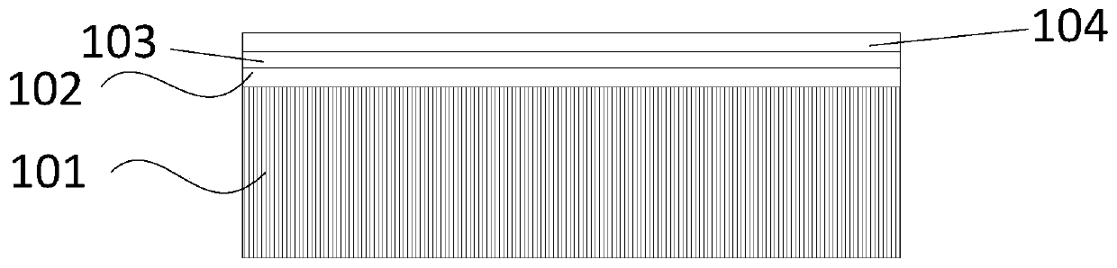
[0061] In the first step, a substrate 101 is provided, which is a bulk silicon substrate 101, and a first hard mask layer, a neutral layer 103 and a second hard mask layer 104 are sequentially deposited on the substrate 101, as figure 2 and image 3 shown.

[0062] Wherein, the hard mask layer The first hard mask layer 102 may be a silicon nitride film, a silicon oxide film, a polysilicon film, an amorphous silicon film, or other suitable hard mask materials, etc. and their stacks. The material of the first hard mask layer 102 can be selected from a material that has a greater selective etching ratio to the material of the layer to be etched. The neutral layer 103 is PS-r-PMMA-HEMA.

[0063] The second hard mask layer 104 may be an amorphous carbon layer, a hard anti-reflection layer or other suitable hard mask materials, etc. and their stacks. The material of the second hard mask layer 104 can be selected from a material that has a greater selective etching ratio between ...


PUM


Abstract

The invention provides a semiconductor structure and a manufacturing method thereof. The manufacturing method comprises the following steps: S1, providing a substrate; S2, forming an induction structure on the surface of the substrate; S3, arranging a first block copolymer layer on the exposed surface of the substrate, and heating the first block copolymer layer for the first time to form a firstpre-split-phase structure layer comprising a first pre-block and a second pre-block; S4, forming at least one second split-phase structure layer on the surface, far away from the substrate, of the first pre-split-phase structure layer; S5, at least removing the fourth block, the second block and part of the substrate in sequence to form the substrate with a predetermined pattern; S6, at least removing the first block, the third block and the induction structure above the remaining substrate. According to the manufacturing method, a phase splitting process is carried out twice, and the manufactured structure has fewer defects, is better in uniformity and is lower in edge roughness.

Description

technical field [0001] The present application relates to the field of semiconductor manufacturing, in particular, to a semiconductor structure and a manufacturing method thereof. Background technique [0002] Photolithography, as the most complex and expensive process in the semiconductor manufacturing process, accounts for more than 35% of the chip manufacturing cost, and takes about 40% to 60% of the entire chip process in terms of time. The minimum pattern size that can be obtained by photolithography directly restricts the development speed of the semiconductor industry. After the commercial lithography machine has crossed the 436nm (G-line), 365nm (I-line), 248nm (KrF) and other wavelength technology generations, the semiconductor industry is currently using 193nm (ArF) immersion lithography plus multiple Exposure technology (MPT, Multiple Patterning Technology) is used to realize the patterning of key structural dimensions in the 22nm, 14nm and even 7nm technology ge...

Claims


Application Information

Patent Timeline
Patent Type & Authority Applications(China)
IPC IPC(8): H01L21/027G03F7/00
Inventor 刘伟晨韦亚一张利斌
Owner INST OF MICROELECTRONICS CHINESE ACAD OF SCI
Why Eureka
Try Eureka