System-in-package structure

a technology of system and packaging, applied in the field of system-in-package, can solve the problems of increasing the size of the chip, the overall cost and yield of the fabrication process, and the stability of the passive device, so as to improve the yield and stability of the ball mounting process

Active Publication Date: 2008-08-26
ADVANCED SEMICON ENG INC
View PDF7 Cites 36 Cited by
  • Summary
  • Abstract
  • Description
  • Claims
  • Application Information

AI Technical Summary

Benefits of technology

[0007]It is therefore an objective of the present invention to provide a package structure having a void in the periphery of a carrier substrate to improve the problem of contamination of solder pads by the flooding of molding compound.
[0009]Preferably, the present invention provides a solder mask having a void therein in the periphery area of a carrier substrate. During the molding process the excess molding compound flushed out from the molding area is able to flow into the void and avoid contaminating the solder pads, thereby improving the yield and stability of the ball mounting process performed on the solder pads thereafter.

Problems solved by technology

However, how to successfully incorporate the complex circuit functions into a single chip has not only increased the fabrication difficulty, but has also increased the size of the chip and the overall cost and yield of the fabrication process.
Consequently, the stability of the passive devices (not shown), active devices (not shown), and solder balls (not shown) disposed on the solder pads 36 is not ideal.

Method used


Image

  • System-in-package structure
  • System-in-package structure
  • System-in-package structure

Examples


Embodiment Construction

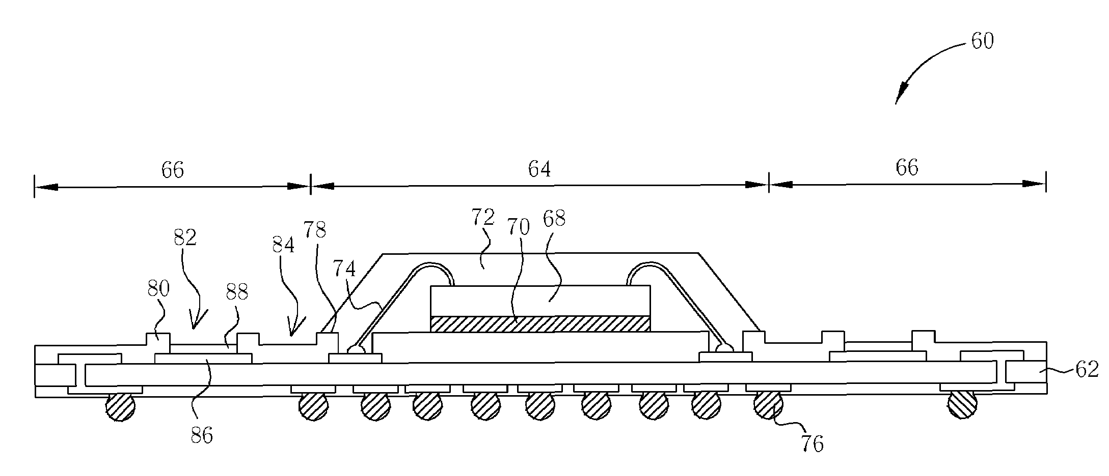
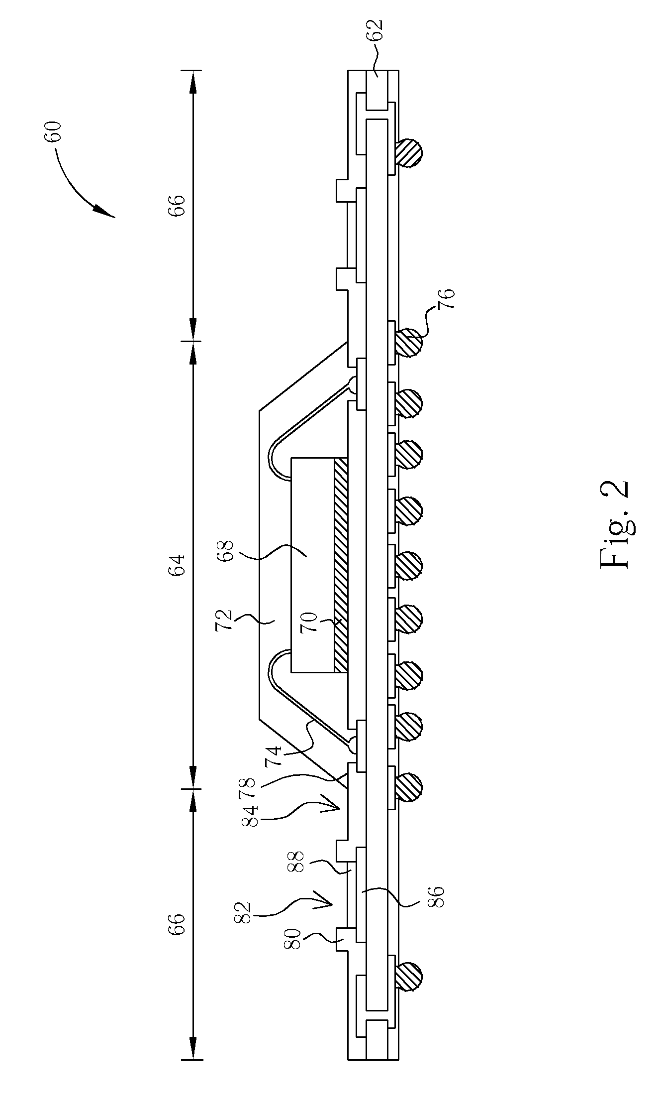
[0014]Please refer to FIG. 2 and FIG. 3. FIG. 2 and FIG. 3 are perspective diagrams illustrating a bottom package structure 60 according to the preferred embodiment of the present invention. As shown in FIG. 2 and FIG. 3, the bottom package structure 60 includes a carrier substrate 62. The surface of the carrier substrate 62 defines a molding area 64 and a periphery area 66, in which the depth of the molding area 64 is greater than the depth of the periphery area 66. The bottom package structure 60 also includes at least a chip 68, positioned on the surface of the carrier substrate 62 and within the molding area 64, an adhesive layer 70 disposed between the carrier substrate 62 and the chip 68, and a molding compound 72 covering the chip 68 and part of the carrier substrate 62. Please note that the chip 68 can be, for example, a flip chip. Additionally, the bottom package structure 60 includes a plurality of wires 74 formed by wire bonding for electrically connecting the chip 68 and...


PUM


Abstract

A system-in-package structure includes a carrier substrate having a molding area and a periphery area, at least a chip disposed in the molding area, an encapsulation covering the chip and the molding area, a plurality of solder pads disposed in the periphery area, and a solder mask disposed in the periphery area and partially exposing the surface of the solder pads. The solder mask includes at least a void therein.

Description

BACKGROUND OF THE INVENTION[0001]1. Field of the Invention[0002]The invention relates to a system-in-package, and more particularly, to a system-in-package having a void in the periphery area of a carrier substrate.[0003]2. Description of the Prior Art[0004]The functionality of electronic products continues to increase, and mirror that is the development of packaging processes. Packaging processes continue a trend toward the high density, miniature size, multi-chip, and three dimensional design. In general, various high density package structures commonly utilized today include wafer level packages, three dimensional packages, multi-chip packages, and system-in-package structures. Preferably, an ideal package structure involves the incorporation of virtually all of the integrated circuits into a silicon chip, such as a system on chip (SoC) design. However, how to successfully incorporate the complex circuit functions into a single chip has not only increased the fabrication difficul...

Claims


Application Information

Patent Timeline
Patent Type & Authority Patents(United States)
IPC IPC(8): H01L23/48H01L29/40H01L23/52
CPCH01L23/3128H05K3/3452H01L25/105H01L23/49811H01L2924/10253H01L2225/107H01L2225/1058H01L2225/1023H01L24/48H05K2203/0588H05K3/284H01L2924/15331H01L2924/15311H01L2224/73265H01L2224/48228H01L2224/48227H01L2224/48091H01L2224/32225H01L2224/16225H01L2924/00014H01L2924/00H01L2924/00012H01L24/73H01L2924/14H01L2224/05573H01L2224/05568H01L2924/181H01L2224/48471H01L2224/05599H01L2224/45099H01L2224/45015H01L2924/207
Inventor CHUANG, MENG-JUNGLEE, CHENG-YINTAI, WEI-CHANGCHU, CHI-CHIH
Owner ADVANCED SEMICON ENG INC
Why Eureka
Try Eureka