Multi-wavelength semiconductor laser

a semiconductor laser and multi-wavelength technology, applied in semiconductor lasers, laser details, electrical equipment, etc., can solve the problems of increasing power consumption, increasing the absorption loss of light, and ar/hr coating alone cannot secure reliability, so as to increase the band gap of the active layer and prevent the absorption of laser light

Active Publication Date: 2008-08-26
PANASONIC SEMICON SOLUTIONS CO LTD
View PDF5 Cites 2 Cited by
  • Summary
  • Abstract
  • Description
  • Claims
  • Application Information

AI Technical Summary

Benefits of technology

[0014]Generally, when a semiconductor laser is caused to perform a high power operation, a resonator end face (front end face) from which laser light is extracted is coated with a dielectric film having a low reflectivity of 10% or less, and a resonator end face (rear end face) on the opposite side is coated with a dielectric film having a high reflectivity of 85% or more. Such coatings of low reflectivity (AR; Anti Reflection) / high reflectivity (HR; High Reflection) make it possible to improve external differential quantum efficiency (slope efficiency) in a current-optical output characteristic, achieve high optical output with a small amount of current injection, reduce the power density of laser light on the front end face during operations, and prevent COD (Catastrophic Optical Damage) in which the optical output of laser light causes melt fracture on the end face of the laser.
[0016]It is therefore thought to be effective to increase the band gap of the active layer near the end face of the laser and prevent the occurrence of COD by diffusing impurity in the active layer on the end face of the laser and causing a quantum well active layer to act as a disordered window region. This is because, even when the band gap of the active layer in the window region near the end face decreases due to heat on the laser during operations, Auger recombination on the end face of the laser, or heat caused by a loss of light absorption in a band, the window region larger in band gap than the active layer causes a transparent state for laser light, that is, the wavelength of laser oscillation light is longer than a wavelength corresponding to the band gap of the window region, and thus absorption of laser light can be prevented in the window region.
[0017]With this window structure, a multi-wavelength semiconductor laser for DVDs and CD-Rs (hereinafter, referred to as a dual wavelength semiconductor laser) can achieve a dual wavelength light source for an optical disc system capable of high-speed writing.
[0021]An object of the present invention is to provide a multi-wavelength semiconductor laser which can facilitate the design of an optical system by means of a window structure in which for a multi-wavelength semiconductor laser device formed on the same substrate, the size of an FFP of laser light at each wavelength is stabilized to obtain a desired FFP pattern.

Problems solved by technology

Even in this case, power consumption increases during operations and heat is generated by an increase in absorption loss of light in the waveguide, so that the band gap of an active layer near the end face of the laser is reduced and laser light is absorbed on the end face of the laser, causing COD.
As a result, the AR / HR coatings alone cannot secure reliability over several thousand hours.

Method used


Image

  • Multi-wavelength semiconductor laser
  • Multi-wavelength semiconductor laser
  • Multi-wavelength semiconductor laser

Examples


Embodiment Construction

[0061]The following will describe an embodiment of the present invention in accordance with the accompanying drawings.

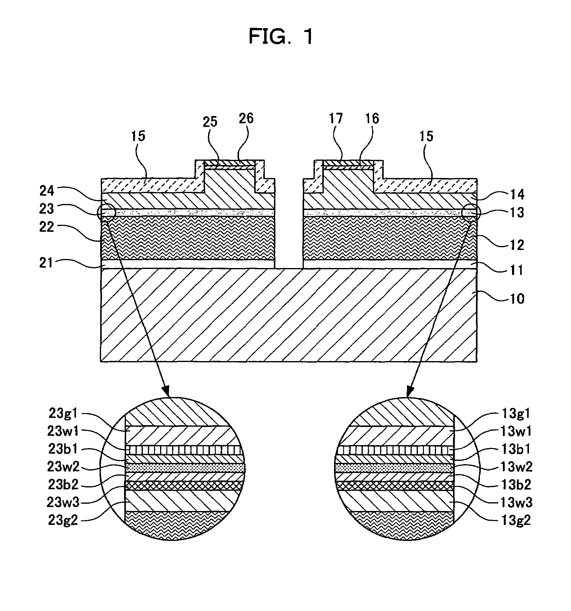
[0062]FIG. 1 is a sectional structural diagram schematically showing a multi-wavelength semiconductor laser of the present invention.

[0063]In this structure, on an n-type GaAs substrate 10 whose principle plane is tilted by 10° from a plane (100) in a direction [011], a red laser and an infrared laser are monolithically integrated. First, the structure of the red laser will be discussed below.

[0064]In the red laser, the following layers are formed: an n-type GaAs buffer layer 11 (0.5 μm), an n-type (Al0.7Ga0.3)0.51In0.49P clad layer 12 (2.0 μm), a strained quantum well active layer 13 including an (Al0.5Ga0.5)0.51In0.49P (500 Å) first guide layer 13g1+[Ga0.48In0.52P (50 Å×3) well layers 13w1 to 13w3+(Al0.5Ga0.5)0.51In0.49P (50 Å×2) barrier layers 13b1 and 13b2]+an (Al0.5Ga0.5)0.51In0.49P (500 Å) second guide layer 13g2, a p-type (Al0.7Ga0.3)0.51In0.49P clad layer 14,...


PUM


Abstract

Semiconductor lasers for respective wavelengths have window regions with different lengths so as to obtain optimum FFPs for emitted light of the respective wavelengths, and thus dependence on optical output can be equal between the wavelengths, facilitating the design of an optical system.

Description

FIELD OF THE INVENTION[0001]The present invention relates to a multi-wavelength semiconductor laser in which semiconductor lasers for a red wavelength, an infrared wavelength, and so on are monolithically formed, the semiconductor laser being used as a light source required for a pickup light source of an optical disk drive, an electronic device, an information processor, and so on.BACKGROUND OF THE INVENTION[0002]Digital video discs (DVDs) allowing high-density recording with a large capacity and DVD devices for reproducing DVDs have been commercially available at present and received attention as products growing in demand. Since DVDs allow high-density recording, AlGaInP semiconductor lasers having an emission wavelength of 650 nm are used as laser light sources for recording / reproducing DVDs. Thus, the optical pickups of conventional DVD devices cannot reproduce compact discs (CDs) and Mini Discs (MDs) which are reproduced using AlGaAs semiconductor lasers having an emission wav...

Claims


Application Information

Patent Timeline
Patent Type & Authority Patents(United States)
IPC IPC(8): H01S5/00
CPCH01S5/162H01S5/40H01S5/22H01S5/4087H01S3/10
Inventor TAKAYAMA, TORUKIDOGUCHI, ISAOKASHIMA, TAKAYUKI
Owner PANASONIC SEMICON SOLUTIONS CO LTD
Why Eureka
Try Eureka