Atomic layer deposition on micro-mechanical devices

a micro-mechanical device and layer deposition technology, applied in the field of micro-mechanical devices, can solve the problems of deformation of silicon during the operation of the mems device, deformation of the micro-mechanical device,

Inactive Publication Date: 2008-09-16
UNIV OF COLORADO THE REGENTS OF
View PDF31 Cites 47 Cited by
  • Summary
  • Abstract
  • Description
  • Claims
  • Application Information

AI Technical Summary

Problems solved by technology

Two significant problems facing MEMS are frictional wear and stiction.
Frictional wear is a common mode of failure and degraded performance for many MEMS.
Silicon may wear significantly during operation of the MEMS device.
Gears and other engaging MEMS components may experience this problem to an even greater extent.
Stiction is another problem facing MEMS.
This self-assembled monolayer approach has a number of limitations.
One limitation is that the coatings are organic and have a very limited range of properties.
The organic coatings do not work well for several surfaces commonly used in MEMS.
Another limitation is that the coatings are limited to a single monolayer, and as such do not provide sufficient electrical insulation, or sufficient protection against frictional wear.
However, CVD has several significant limitations that render it generally unsuitable for MEMS.
One limitation is that the high deposition temperatures for CVD are often not suitable for MEMS.
Differences in coefficients of thermal expansion between the deposition layer and underlying materials, over the large temperature range between deposition temperature and ambient, may create significant material stresses between the deposition layer and underlying materials.
Another limitation is that the deposited layers do not have uniform thickness.
Accordingly, prior art methods for depositing layers on MEMS have a number of significant limitations and improved systems and methods for depositing layers on MEMS are needed.

Method used


Image

  • Atomic layer deposition on micro-mechanical devices
  • Atomic layer deposition on micro-mechanical devices
  • Atomic layer deposition on micro-mechanical devices

Examples


example 1

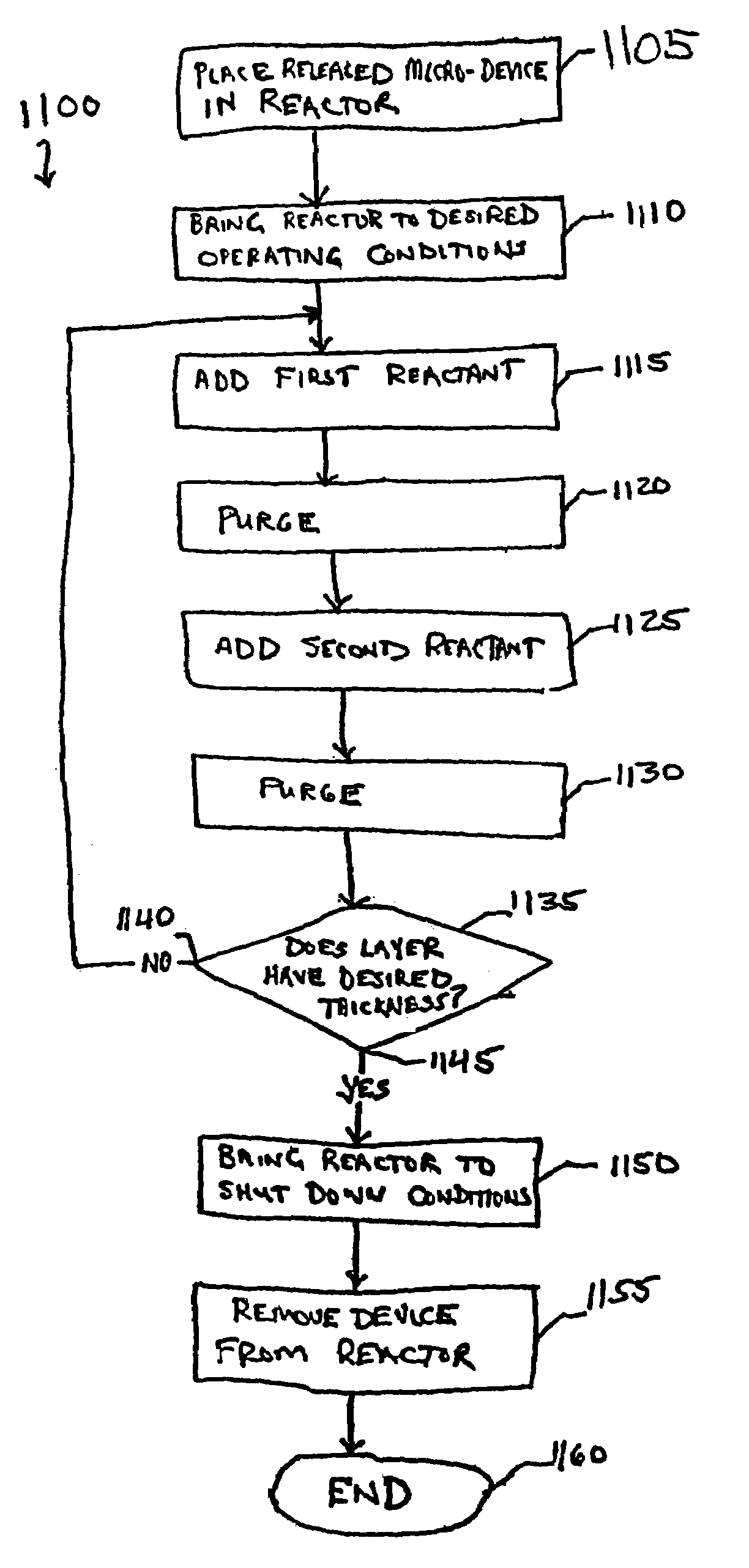
Depositing a Frictional Wear Reducing Layer on a Micro-Mechanical Device

[0092]ALD may be used to deposit materials suitable to reduce frictional wear on micro-mechanical devices. This may be achieved by depositing a layer comprising a material having a hardness, wear-resistance, coefficient of friction, or other material characteristic more favorable than that of at least a portion of the device to protect moving parts from frictional wear and increase the life of the device. For example, the device may comprise a first silicon portion having a hardness of about 10-12 GPa (about 7 on the Mohs hardness scale) to contact a second silicon portion having a similar hardness and the deposited layer may comprise a material sufficiently harder than silicon deposited on the first portion and the second portion. Advantageously, the layer may contact on behalf of the first portion and the second portion and may reduce wear due to the greater hardness. For example, the material deposited may co...

example 2

Depositing an Electrically Insulating Layer on a Micro-Electromechanical Device

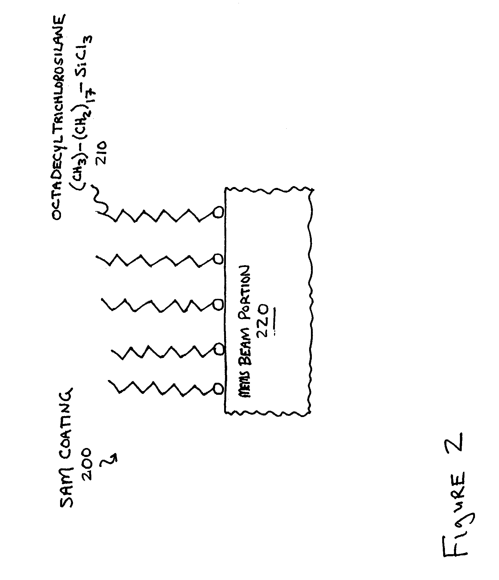
[0093]ALD may be used to deposit materials suitable to reduce electrical shorting in micro-electromechanical devices. This may be achieved by depositing a layer that comprises a material or materials that have sufficient electrical properties to prevent electrical shorting between proximate electrical components or between proximate devices. This may be done by depositing a material that is sufficiently dielectric (i.e., provides sufficient electrical insulation) or that has a sufficient electrical resistance to prevent electrical shorting.

[0094]Consider a micro-mechanical device that has a first silicon portion to contact a second proximate silicon portion. Silicon has particular electrical properties including a dielectric constant of about 11-12 and an electrical resistance of about 1 Ohm*cm for doped silicon. Such electrical properties may lead to an electrical shorting tendency that may be reduced by...

example 3

Exemplary Device Having a Wear Reducing and Electrically Insulating Layer

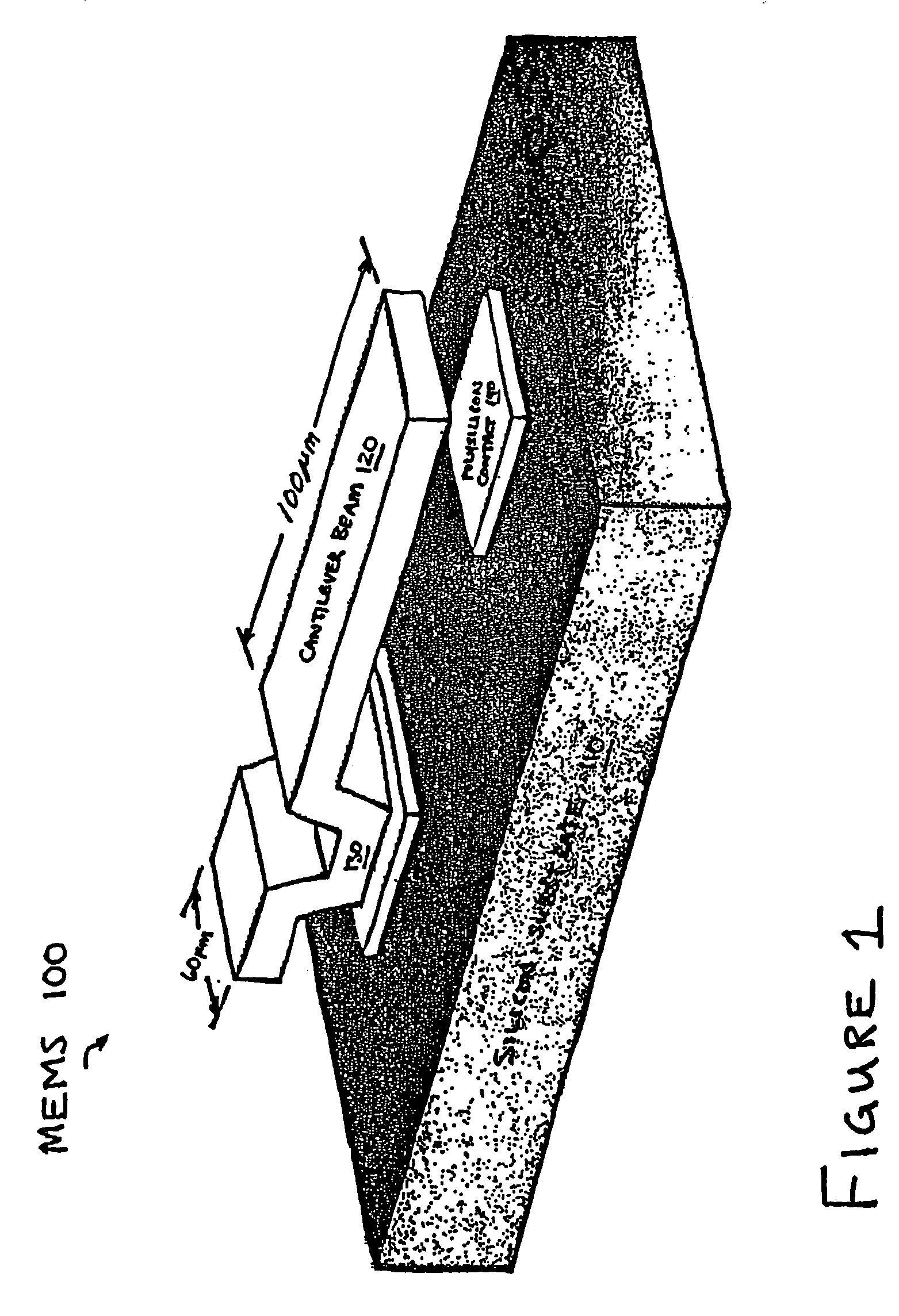
[0095]FIG. 13 shows a side view of a cantilever MEMS 1300 having a layer of Al2O3 deposited thereon by ALD. According to one embodiment, the layer may be deposited by the method of FIG. 11. Advantageously, the layer of Al2O3 may be sufficiently hard to reduce frictional wear to the MEMS 1300 and sufficiently dielectric to reduce electrical shorting to the MEMS 1300.

[0096]The device 1300 includes a cantilever beam 1320 having a bottom surface 1321 and enclosing a void 1370, a first polysilicon contact plate 1340, an anchor 1330 to fixedly attach the beam 1320 to the plate 1340, a second polysilicon contact plate 1340, a silicon substrate 1310 fixedly attached with the first plate 1340 and the second plate 1350, and a layer of Al2O3 1390 deposited conformally and in substantially uniform thickness to an exposed outer surface of the device 1300 including the bottom surface 1321 and a housing of the void 1370. Adva...


PUM


Abstract

A micro-electromechanical device or MEMS having a conformal layer of material deposited by atomic layer deposition is discussed. The layer may provide physical protection to moving components of the device, may insulate electrical components of the device, may present a biocompatible surface interface to a biological system, and may otherwise improve such devices. The layer may also comprise a combination of multiple materials each deposited with great control to allow creating layers of customizable properties and to allow creating layers having multiple independent functions, such as providing physical protection from wear and providing electrical insulation.

Description

RELATED APPLICATIONS[0001]The present application is a continuation-in-part of and claims priority to and fully incorporates herein U.S. Provisional Patent Application Ser. No. 60 / 341,486, entitled “ATOMIC LAYER DEPOSITION ON MICRO-MECHANICAL DEVICES”, by Bright et al., filed on Dec. 17, 2001; and the present application is a continuation-in-part of and claims priority to and fully incorporates herein U.S. Provisional Patent Application Ser. No. 60 / 385,225, entitled “ATOMIC LAYER DEPOSITION ON MICRO-MECHANICAL DEVICES”, by Bright et al., filed on May 31, 2002.STATEMENT OF GOVERNMENT RIGHTS[0002]The present invention was made with United States government support under Grant Number F49620-99-1-0081 awarded by the Air Force Office Of Scientific Research, Grant Number F33615-98-C-5429 awarded by the Air Force Research Laboratory, and Grant Number DGE-9870665 awarded by the National Science Foundation. The government has certain rights in the invention.COPYRIGHT NOTICE[0003]Contained he...

Claims


Application Information

Patent Timeline
Patent Type & Authority Patents(United States)
IPC IPC(8): G02B26/08
CPCB81B3/0005B81C1/0096B81C1/00674B81B2207/115B81C2201/112Y10S359/90
Inventor BRIGHT, VICTOR M.ELAM, JEFFREYFABREGUETTE, FRANCOISGEORGE, STEVEN M.HOIVIK, NILSLEE, YUNG-CHENGLINDERMAN, RYANTRIPP, MARIE
Owner UNIV OF COLORADO THE REGENTS OF
Why Eureka
Try Eureka