
Method and apparatus for inspecting defects in multiple regions with different parameters

a defect and parameter technology, applied in the field of defect inspection, can solve the problems of hundreds to thousands of defects detected on the semiconductor substrate, generating the above-mentioned defects on the pattern, and reducing the review time, so as to accurately classify the defects

Active Publication Date: 2008-10-07
SAMSUNG ELECTRONICS CO LTD
View PDF12 Cites 2 Cited by
  • Summary
  • Abstract
  • Description
  • Claims
  • Application Information

AI Technical Summary

Benefits of technology

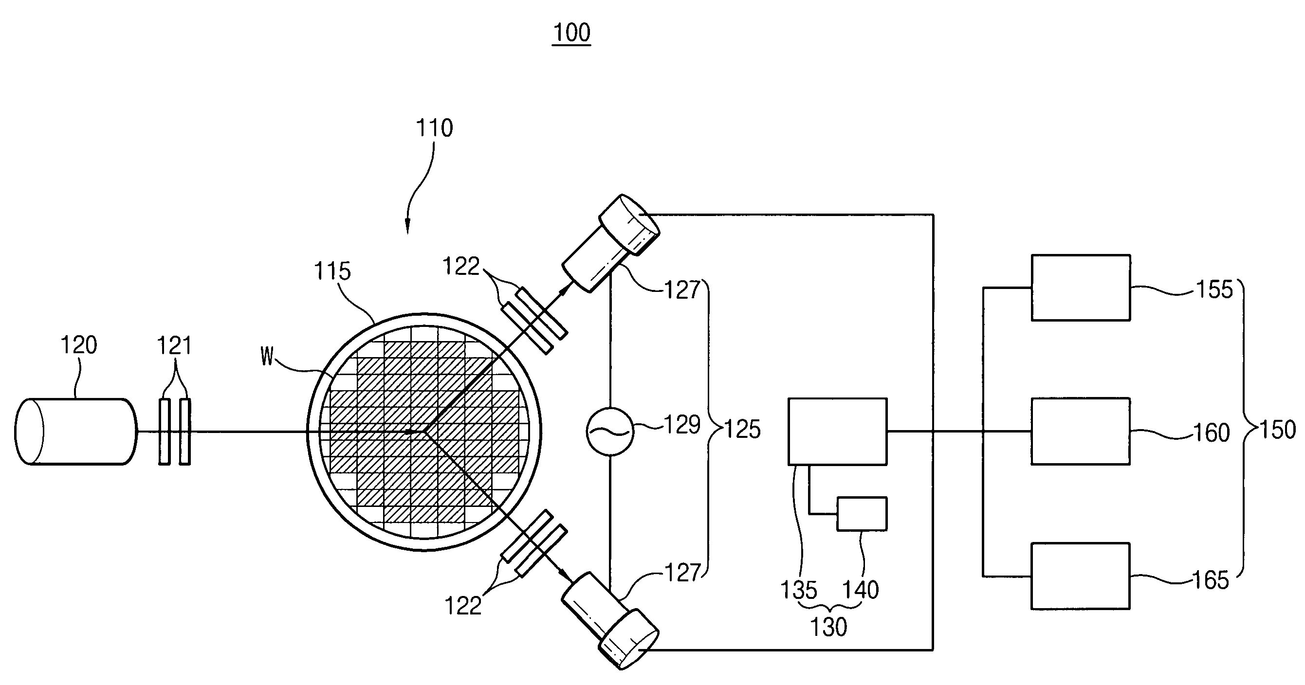
The present invention provides a method and apparatus for inspecting defects on an object using a light-based approach. The method involves illuminating an object and collecting light from different regions of the object based on different characteristic parameters. The collected light is then analyzed to determine if any abnormal defects exist. This process allows for more accurate classification of defects without the need for a separate inspection tool. The apparatus includes a scanning unit for scanning the object and a determining unit for identifying points where the object is changed from one region to another. The inspecting unit then inspects the information based on the characteristic parameters to detect and classify defects on the object. This method and apparatus can significantly reduce the time required for reviewing defects.

Problems solved by technology

For example, after a pattern is formed on a semiconductor substrate, defects such as particles or micro-scratches may be generated on the pattern.
Planarization of the pattern by a chemical mechanical polishing (CMP) process may also generate the above-mentioned defects on the pattern.
With increased integration, however, hundreds to thousands of inspection regions are set on a single semiconductor substrate resulting in hundreds to thousands of defects detected on the semiconductor substrate.
The increased number of required inspections has resulted in a skyrocketing time to complete the inspection of the semiconductor devices.
Critical defects are recognized during this manual inspection process.
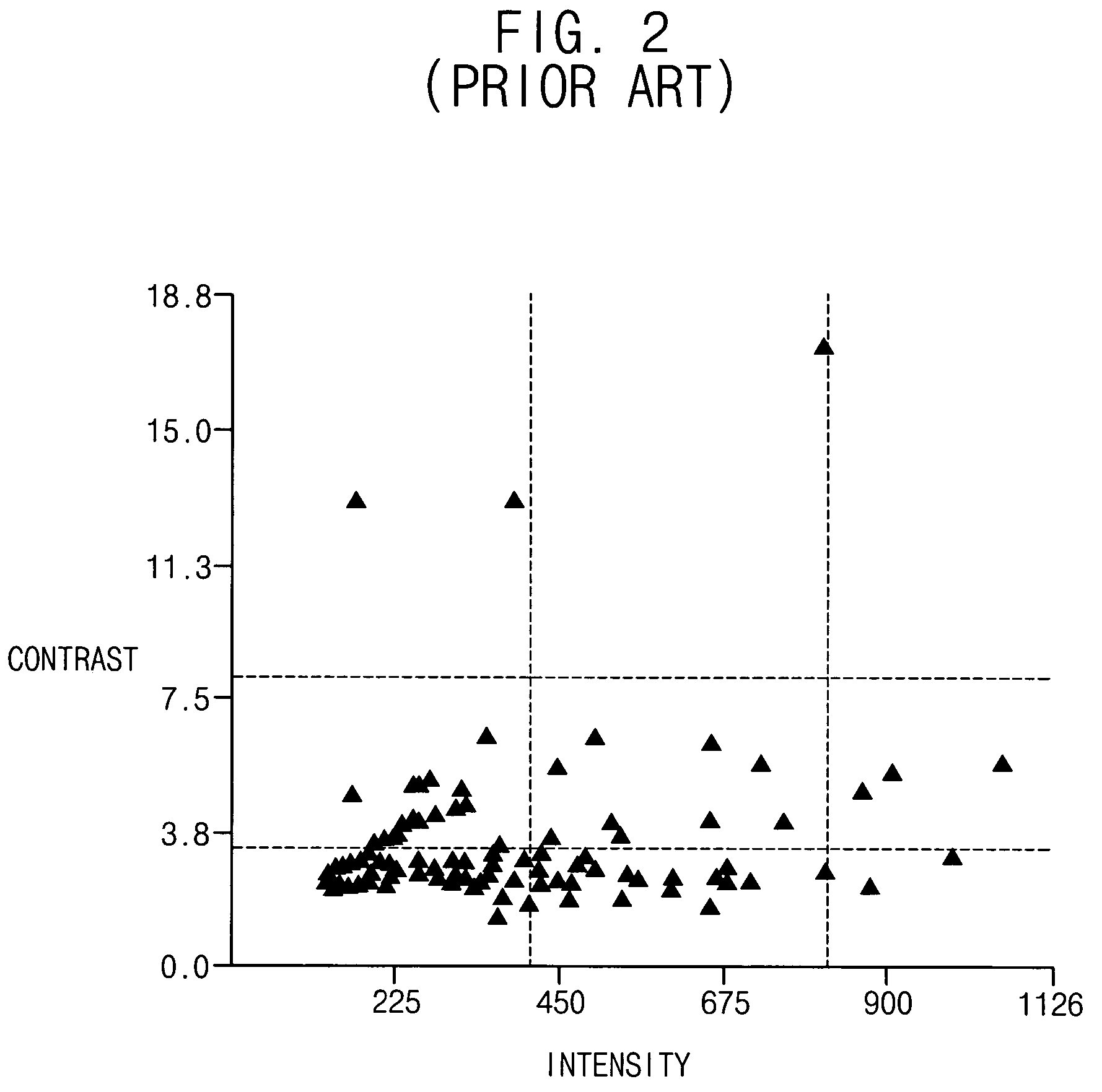
It has been found, however, that defects with diverse contrasts and intensities may actually be of a similar type and that those defects with similar contrasts and intensities may in fact be quite different types of defects—a fact that cannot be determined from a simple inspection of the conventional contrast / intensity plot as shown in FIG. 2.
That is, defects having the above-mentioned conditions are not adequately distinguished from each other.
According to the conventional method, since the defects detected from entire regions of a semiconductor substrate are classified based on the same parameters, the conventional defect classification has a very low accuracy.
Thus, defect inspection under the conventional method requires a further manual inspection to determine whether the critical defects found would be of the type that would influence subsequent processing or operation.
Accordingly, the time required to conduct inspections of the devices increases thus also increasing a cost for manufacturing the semiconductor device.
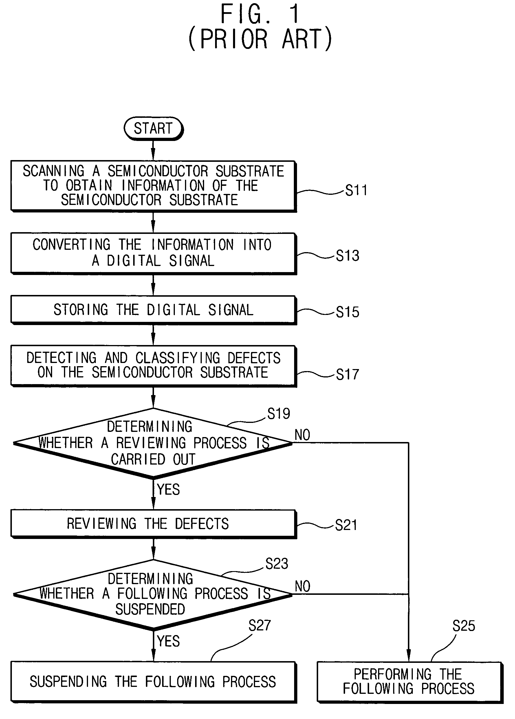
An image of the semiconductor substrate is obtained using an SEM, a typically time intensive procedure.
That is, since the SEM is used in the conventional method, efficiency for detecting defects is very low.
And although the regions have similar densities, the regions may in fact have different kinds defects so that the defect classification is relatively inaccurate.
Thus, a reviewing of the defects is required in the conventional method resulting in the original problem.

Method used


Image

  • Method and apparatus for inspecting defects in multiple regions with different parameters
  • Method and apparatus for inspecting defects in multiple regions with different parameters
  • Method and apparatus for inspecting defects in multiple regions with different parameters

Examples


Embodiment Construction

[0036]The present invention is described more fully hereinafter with reference to the accompanying drawings, in which embodiments of the invention are shown. This invention may, however, be embodied in many different forms and should not be construed as limited to the embodiments set forth herein. Rather, these embodiments are provided so that this disclosure will be thorough and complete, and will fully convey the scope of the invention to those skilled in the art. In the drawings, the sizes and relative sizes of layers and regions may be exaggerated for clarity.

[0037]It will be understood that when an element or layer is referred to as being “on”, “connected to” or “coupled to” another element or layer, it can be directly on, connected or coupled to the other element or layer or intervening elements or layers may be present. In contrast, when an element is referred to as being “directly on,”“directly connected to” or “directly coupled to” another element or layer, there are no int...


PUM

PropertyMeasurementUnit
wavelengthaaaaaaaaaa
incident angleaaaaaaaaaa
dark currentaaaaaaaaaa

Abstract

In a method of inspecting defects, a first actual region of an actual object is inspected based on a first characteristic parameter as an inspection condition. A point where an inspection region of the actual object is changed into a second actual region from the first actual region is determined. The second actual region is then inspected based on a second characteristic parameter as the inspection condition. The first and second parameters may include contrast of a light that is reflected from a reference object, intensity of the light, brightness of the light, a size of a minute structure on the reference object, etc. The characteristic parameters of each reference region on the reference object are set. Thus, the defects may be accurately classified so that a time and a cost for reviewing the defects may be markedly reduced.

Description

BACKGROUND OF THE INVENTION[0001]1. Cross-References to Related Applications[0002]This application claims priority under 35 USC § 119 to Korean Patent Application No. 2004-83401, filed on Oct. 19, 2004, the contents of which are herein incorporated by reference in its entirety for all purposes.[0003]2. Field of the Invention[0004]The present invention relates to a method of inspecting defects and an apparatus for performing the same. More particularly, the present invention relates to a method of inspecting defects that is capable of detecting the defects on a precision object such as a semiconductor substrate and then classifying the defects, and an apparatus for performing the method.[0005]3. Description of the Prior Art[0006]Continued improvements in semiconductor design and manufacturing result in devices having ever increasing integration and capacity. Such devices require extremely accurate thin layer patterns to be formed on the semiconductor substrate, and such accuracy is d...

Claims


Application Information

Patent Timeline
Patent Type & Authority Patents(United States)
IPC IPC(8): G01B15/00G01N21/00
CPCG01N21/21G01N21/95607G01N21/47H01L22/00
Inventor KIM, JOUNG-SOOCHON, SANG-MUNJUN, CHUNG-SAMYANG, YU-SIN
Owner SAMSUNG ELECTRONICS CO LTD
Learn More