Frequency-doubled edge-emitting semiconductor lasers

a laser and semiconductor technology, applied in semiconductor lasers, laser cooling arrangements, laser details, etc., can solve the problems of complex free-space optics, inability to achieve a focused free-space beam with a high intensity, and no commercially available diode lasers, etc., to facilitate coupling the fundamental radiation

Inactive Publication Date: 2008-10-07
COHERENT INC
View PDF31 Cites 6 Cited by
  • Summary
  • Abstract
  • Description
  • Claims
  • Application Information

AI Technical Summary

Problems solved by technology

There are no commercially available diode-lasers that emit fundamental radiation at any wavelength between the red and blue regions of the visible electromagnetic spectrum.
Such an extended path with a high intensity is not achievable with a focused free-space beam.
A problem with this approach is that complex free-space optics are needed to launch the diode-laser output into the PP crystal.
This generates additional problems due to a requirement for precise alignment and a high degree of mechanical stability.
This also drives the cost of such a frequency-doubled diode-laser beyond a level tolerable in most applications.
While relatively inexpensive, these lasers are still somewhat vulnerable to misalignment by mechanical shock or temperature cycling.

Method used


Image

  • Frequency-doubled edge-emitting semiconductor lasers
  • Frequency-doubled edge-emitting semiconductor lasers
  • Frequency-doubled edge-emitting semiconductor lasers

Examples


Embodiment Construction

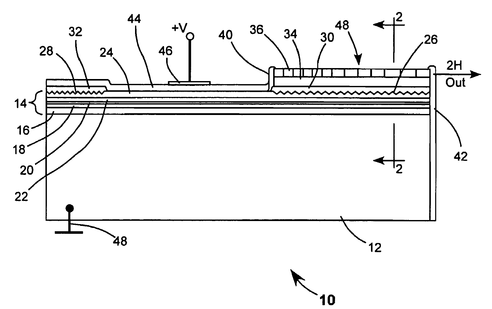
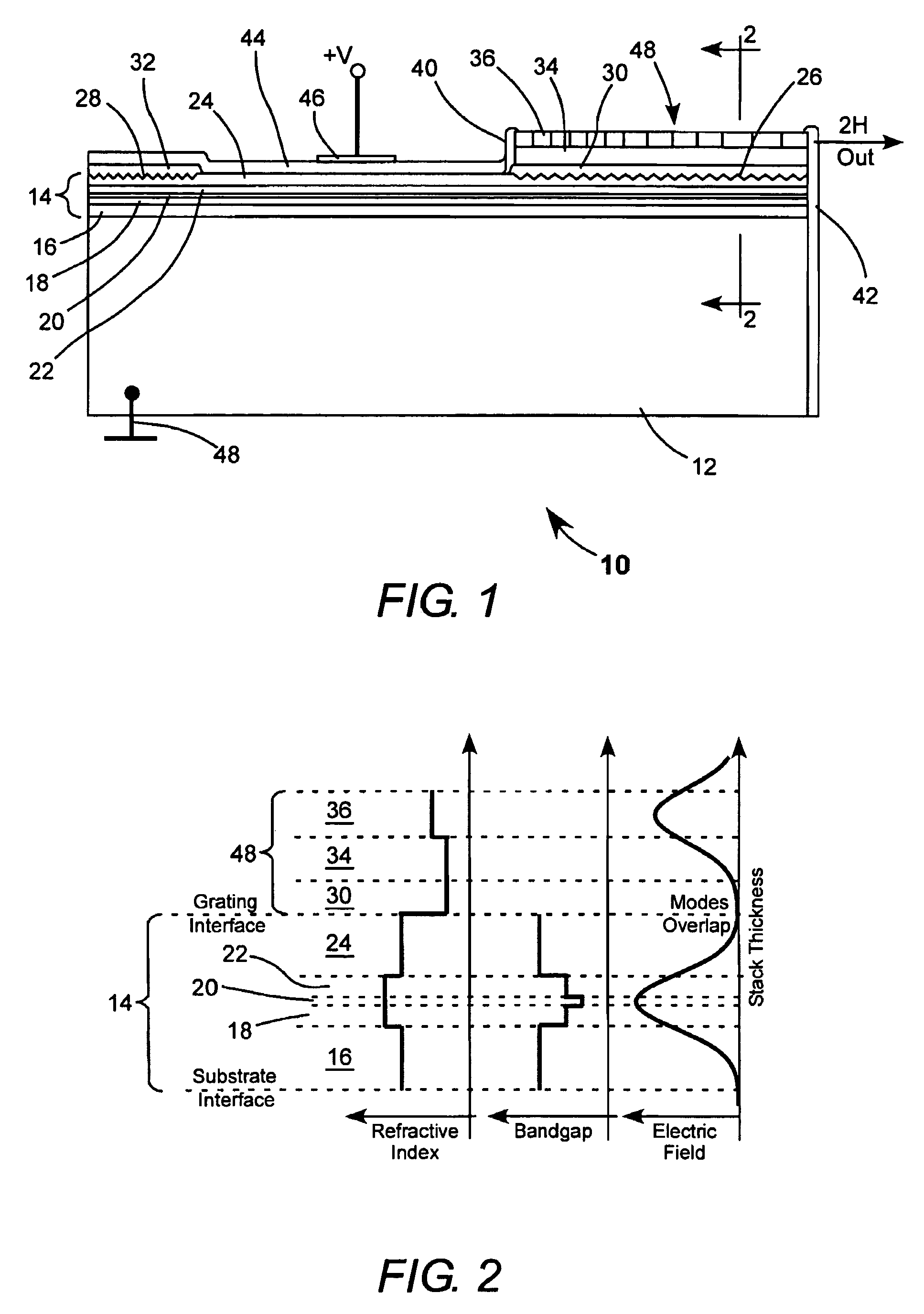
[0020]Referring now to the drawings, wherein like components are designated by like reference numerals, FIG. 1 is an un-shaded longitudinal cross-section view schematically illustrating one preferred embodiment 10 of a frequency-doubled diode-laser in accordance with the present invention. FIG. 2 schematically graphically represents a refractive index profile, bandgap profile, and an electric-field intensity profile in frequency doubled diode-laser 10 seen generally in the direction 2-2 of FIG. 1.

[0021]Laser 10 includes a single crystal substrate 12 on which is an epitaxially grown, separate-confinement semiconductor heterostructure 14. In this example, heterostructure 14 includes a lower cladding layer 16, a lower waveguide layer 18, a quantum-well layer 20, an upper waveguide layer 22, and an upper cladding layer 24. Layers of heterostructure 14 are preferably layers of various formulations of III-V materials. The relative refractive index and bandgap of the layers, whatever the m...


PUM


Abstract

A frequency-doubled, edge-emitting semiconductor laser includes a separate confinement heterostructure surmounted by a waveguide including a converting layer of a periodically poled, optically nonlinear material. Fundamental radiation generated in the heterostructure is directionally coupled from the heterostructure into the waveguide, is converted to second-harmonic radiation in the converting layer and is delivered from the waveguide as output radiation. In one example, a distributed Bragg grating is included at an interface between the heterostructure and the waveguide for facilitating coupling of fundamental radiation from the heterostructure into the waveguide.

Description

TECHNICAL FIELD OF THE INVENTION[0001]The present invention relates in general to edge-emitting semiconductor lasers. The invention relates in particular to frequency-doubling fundamental radiation of electrically pumped, edge-emitting semiconductor lasers (diode-lasers) and optically pumped, edge-emitting semiconductor lasers.DISCUSSION OF BACKGROUND ART[0002]Compact, robust and inexpensive laser sources of visible light have many applications in consumer products, industrial processes and scientific instruments. Electrically pumped, edge-emitting semiconductor lasers, usually referred to by practitioners of the art as diode-lasers, are compact, robust and efficient. However, the most common commercially-available diode-lasers are lasers that emit light in the red region of the visible electromagnetic spectrum or the near infrared (NIR) region of the invisible electromagnetic spectrum. A few commercial suppliers are able to provide diode-lasers that emit fundamental radiation in th...

Claims


Application Information

Patent Timeline
Patent Type & Authority Patents(United States)
IPC IPC(8): H01S3/10
CPCH01S5/026H01S5/0604H01S5/1032H01S5/4031H01S5/028H01S5/041H01S5/125H01S5/3211
Inventor GOVORKOV, SERGEI V.AUSTIN, R. RUSSEL
Owner COHERENT INC
Why Eureka
Try Eureka