Non-volatile memory system having a pseudo pass function

a memory system and function technology, applied in memory systems, digital storage, instruments, etc., can solve the problems of data not being correctly written or erased, the threshold value of a certain memory cell suddenly becomes high, and there is no effective way to prevent sudden bit errors at presen

Inactive Publication Date: 2008-10-07
KK TOSHIBA
View PDF11 Cites 99 Cited by
  • Summary
  • Abstract
  • Description
  • Claims
  • Application Information

AI Technical Summary

Problems solved by technology

According to the phenomenon, the threshold value of a certain memory cell suddenly becomes high; as a result, data is not correctly written or erased.
However, sudden bit error is possibly related to the aging degradation of a memory cell.
Judging from the peculiarity described above, sudden bit error is not a phenomenon which happens resulting from fatal failure of the memory cell, but is considered a soft error.
There exists no way to effectively prevent sudden bit error at present.
Sudden bit error occurs in non-volatile semi-conductor memory devices using the same non-volatile memory cell as NAND flash memory regardless of the NAND flash memory.
There is a possibility of a serious problem arising in a multi-value memory having a data corresponding threshold distribution range severer than a normal two-value memory.
More specifically, even if the bit error occurs when a chip internal write or erase sequence is completed, ECC is carried out in a system or flash controller in the read operation.
As a result, there is a problem that available memory capacity is easily reduced.

Method used


Image

  • Non-volatile memory system having a pseudo pass function
  • Non-volatile memory system having a pseudo pass function
  • Non-volatile memory system having a pseudo pass function

Examples


first embodiment

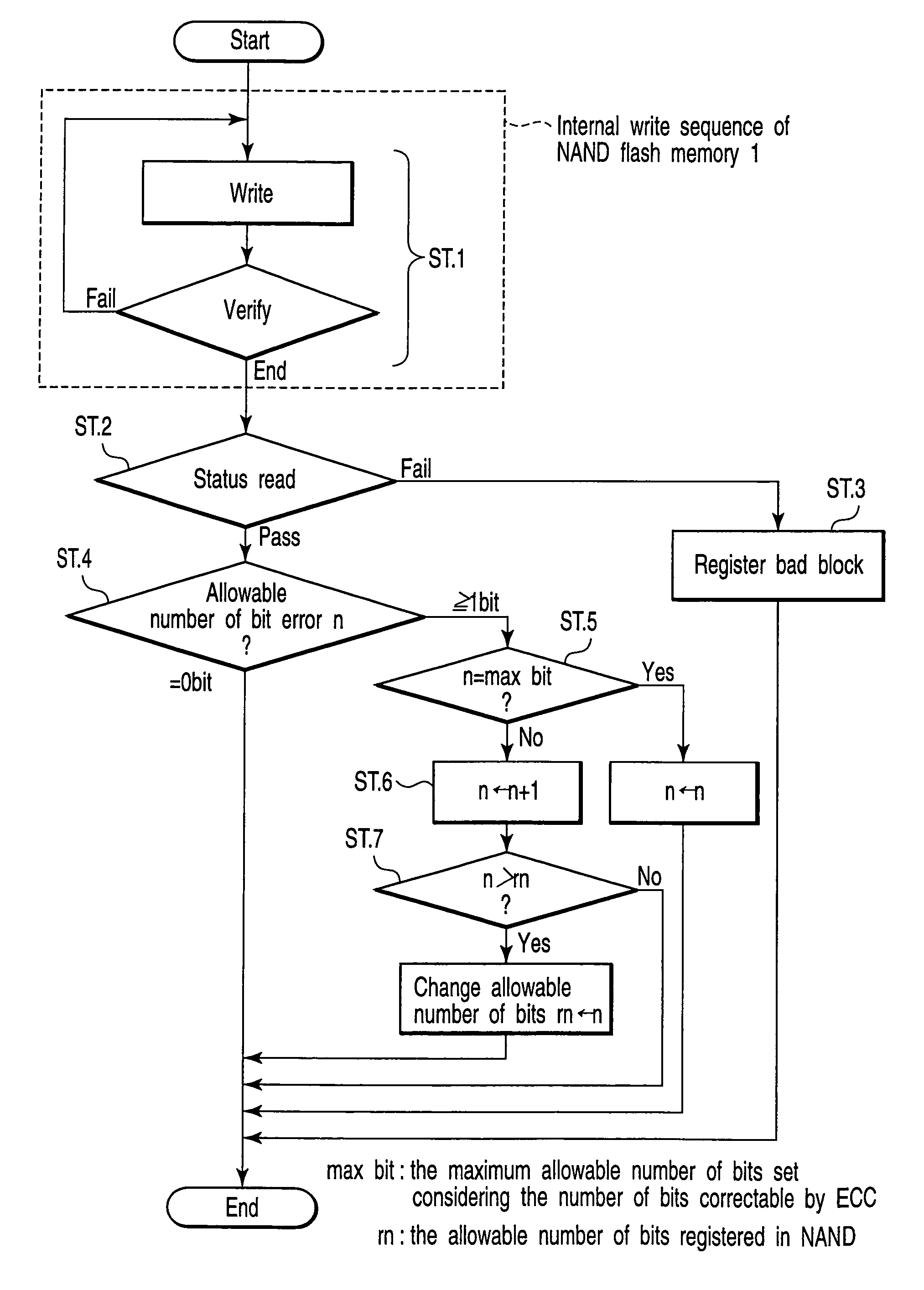
[0036]In a non-volatile memory, for example, a NAND flash memory, the state of a memory cell is automatically verified in the chip during a chip internal write or erase sequence. The following is an explanation of the case where the chip internal write sequence is carried out. The chip internal erase sequence is carried out in the same manner as above.

[0037]The write operation is carried out using a page as the unit. Each bit line is connected with a data register, and data equivalent to one page is loaded into the data register at the beginning of the write operation. The write is divided several times, and then, the state of the memory cell is verified together with data included in the data register. The chip internal write sequence ends in the following cases. One is the case where it is confirmed according to the verify operation that a write to all memory cells of the page is completed. Another is the case where the write time exceeds a predetermined time. Another is the case ...

second embodiment

[0068]FIG. 7 is a block diagram showing the configuration of a non-volatile memory system according to a second embodiment of the present invention.

[0069]As shown in FIG. 7, a controller 3 used in the second embodiment includes a count section for counting the number of rewrite times of the memory 1. A counter is given as one example of the count section, and calls a rewrite counter 21 in this second embodiment.

[0070]In the memory cell of the memory 1, its write performance is reduced gradually with an increase of the number of data rewrite times. As a result, the probability of causing sudden bit error becomes high. Conventionally, in the memory 1 having the pseudo pass function, the same allowable number of bits is applied all over the period from the delivery to the use. Considering the entirety of the non-volatile memory system including the controller 3, a block such that several sudden bit errors occur in one page is registered as a bad block in the delivery, and then, should ...

third embodiment

[0083]According to the foregoing embodiments, the allowable number of bits rn is stored in the ROM fuse 13. The allowable number of bits rn may be stored in forms other than the ROM fuse 13. The third embodiment relates to one example of storing the allowable number of bits rn in forms other than the ROM fuse 13.

[0084]According to the third embodiment, the allowable number of bits rn is stored in part of a page of a block. FIG. 9 is a view to explain the relationship between block and page.

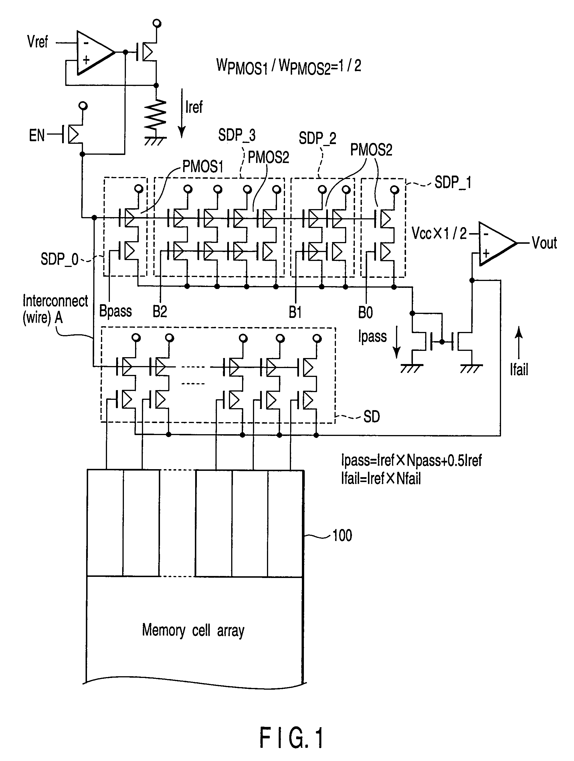
[0085]As illustrated in FIG. 9, the memory cell array 15 includes 1024 blocks BLOCK0 to BLOCK1023. The block is used as the smallest unit for an erase. One block BLOCK includes 4256 NAND memory units. The NAND memory unit includes series-connected several non-volatile semiconductor memory cell-transistors M, for example, four memory cell transistors M. The NAND memory unit further includes a select gate transistor S1 connected to one terminal of series-connected four memory cell transistors M, and...


PUM


Abstract

A non-volatile memory system comprises a non-volatile memory and a memory controller controlling the non-volatile memory. The non-volatile memory has a pseudo pass function of returning a pass as a status even if a bit error reaching allowable number of bits occurs after at least one of a write or erase sequence is completed. The memory controller has an allowable bit change function of changing the upper limit value of the allowable number of bits.

Description

CROSS-REFERENCE TO RELATED APPLICATIONS[0001]This application is based upon and claims the benefit of priority from prior Japanese Patent Application No. 2004-322718, filed Nov. 5, 2004, the entire contents of which are incorporated herein by reference.BACKGROUND OF THE INVENTION[0002]1. Field of the Invention[0003]The present invention relates to a non-volatile memory system, and in particular, to a non-volatile memory system having a pseudo pass function.[0004]2. Description of the Related Art[0005]If a non-volatile semiconductor memory device, for example, NAND flash memory, is used, bit error detection and correction by error checking and correcting (ECC) are effective for ensuring sufficient reliability. For example, a standard system using a multi-value NAND flash memory has a built-in ECC, which enables four-symbol bit error detection and correction per page.[0006]High integration and large capacity have advanced in the NAND flash memory. In a NAND flash memory having such hi...

Claims


Application Information

Patent Timeline
Patent Type & Authority Patents(United States)
IPC IPC(8): G06F11/00
CPCG06F11/1068G11C29/52G11C29/832G11C2029/0411
Inventor SUGIURA, YOSHIHISATANAKA, TATSUYAINOUE, ATSUSHI
Owner KK TOSHIBA
Why Eureka
Try Eureka