
Flash memory device for performing bad block management and method of performing bad block management of flash memory device

a flash memory device and bad block technology, applied in the field of nonvolatile semiconductor memory devices, can solve the problems of reducing the time required for managing defective blocks, and reducing the complexity of firmwar

Inactive Publication Date: 2008-10-07
SAMSUNG ELECTRONICS CO LTD
View PDF11 Cites 94 Cited by
  • Summary
  • Abstract
  • Description
  • Claims
  • Application Information

AI Technical Summary

Benefits of technology

The present invention provides a flash memory device and method for managing defective blocks at a hardware level, which speeds up the process and reduces complexity. The device includes a memory cell array unit, a bad block mapping register, an address comparator, and a bad block-state controller. The method involves receiving a logical address, determining a count number of a re-mapping mark, and selecting a reserved block address or providing the logical address to the memory cell array unit based on the count number. This reduces the time and complexity of managing defective blocks and improves the efficiency of the flash memory device.

Problems solved by technology

As the integration density of integrated flash memory devices has increased, it has become more difficult to fabricate integrated circuit memory devices that are completely free of defective memory cells.
According to the conventional defective block management, the firmware has excessively many commands (or codes) that provide addresses and change the defective block address to a new address.
In addition, according as the firmware codes are more complex, total performance of system using the flash memory device may be further degraded.

Method used


Image

  • Flash memory device for performing bad block management and method of performing bad block management of flash memory device
  • Flash memory device for performing bad block management and method of performing bad block management of flash memory device
  • Flash memory device for performing bad block management and method of performing bad block management of flash memory device

Examples


Embodiment Construction

[0032]Detailed illustrative embodiments of the present invention are disclosed herein. However, specific structural and functional details disclosed herein are merely representative for purposes of describing exemplary embodiments of the present invention. This invention may, however, be embodied in many alternate forms and should not be construed as limited to the embodiments set forth herein.

[0033]Accordingly, while the invention is susceptible to various modifications and alternative forms, specific embodiments thereof are shown by way of example in the drawings and will herein be described in detail. It should be understood, however, that there is no intent to limit the invention to the particular forms disclosed, but on the contrary, the invention is to cover all modifications, equivalents, and alternatives falling within the spirit and scope of the invention. Like numbers refer to like elements throughout the description of the figures.

[0034]It should also be noted that in som...


PUM


Abstract

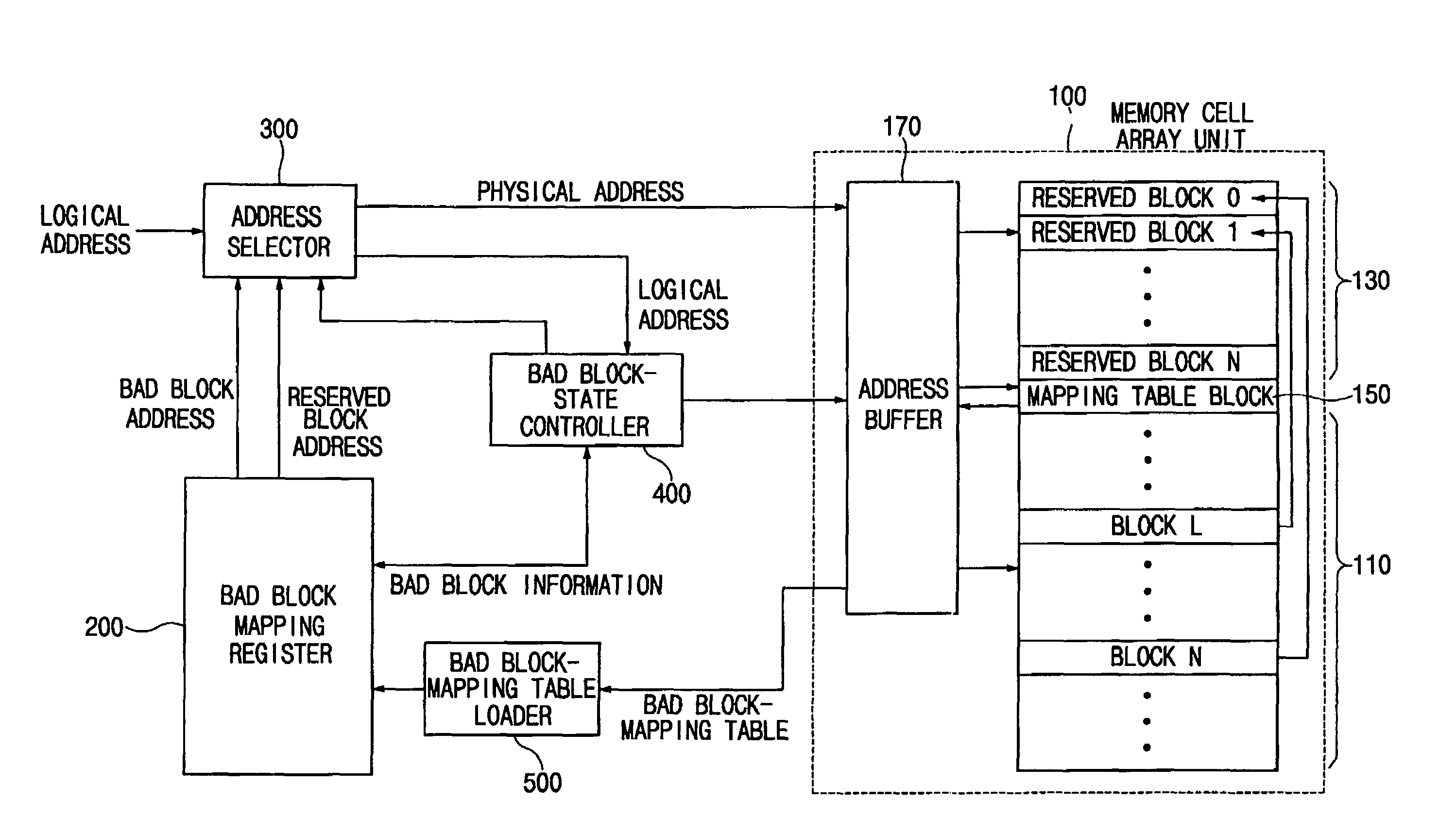
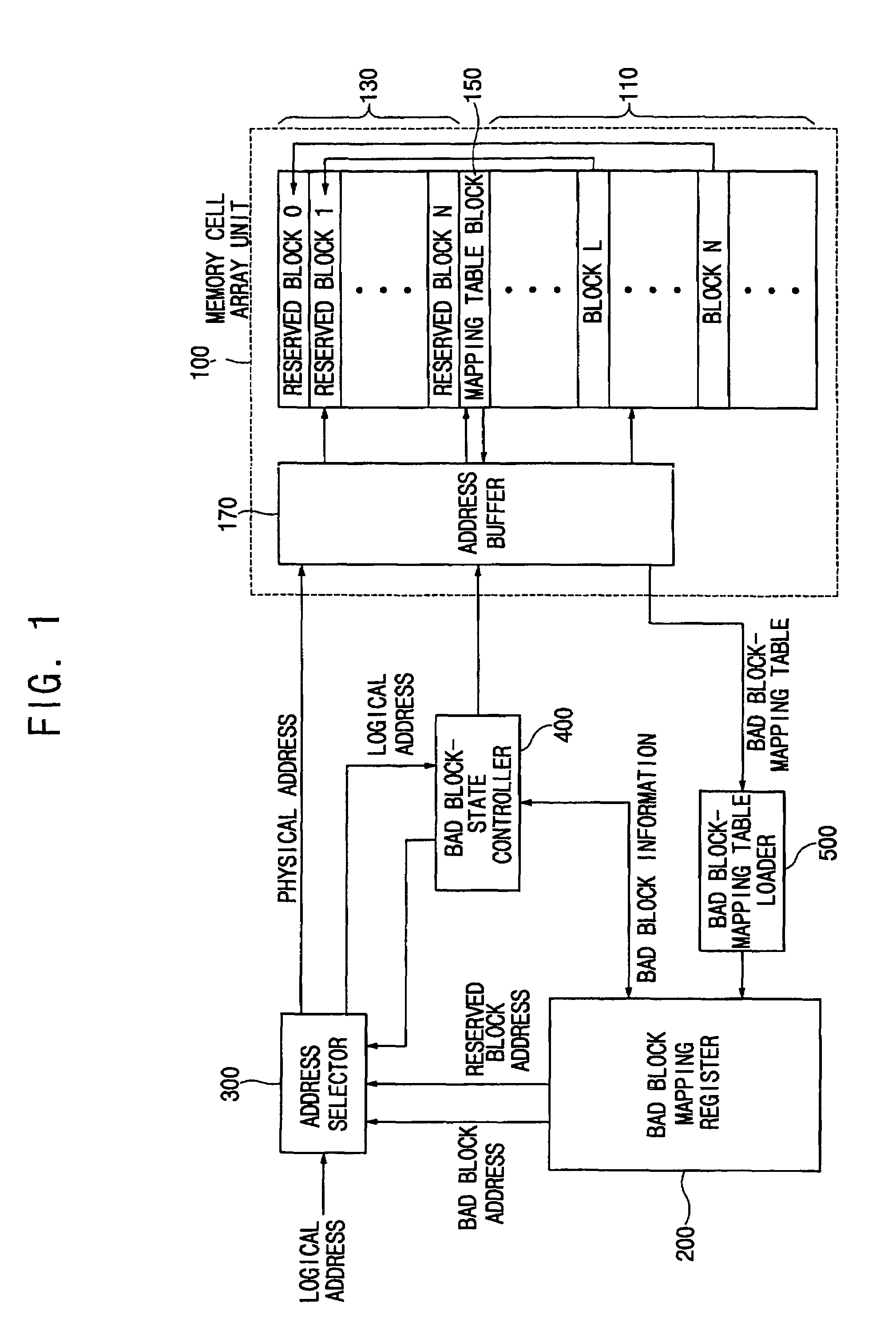
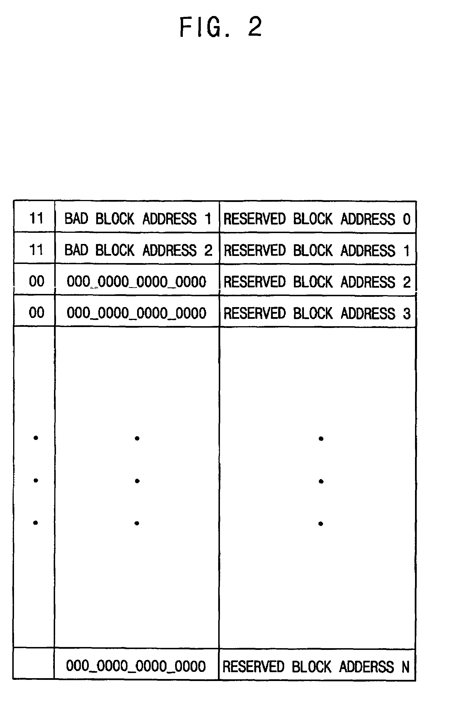
A flash memory device for performing a bad block management and a method of performing bad block management are implemented in hardware level. During a booting procedure of a flash memory device, a bad block-mapping table stored in a predetermined block of memory cell array unit or other nonvolatile memory is stored in a bad block mapping register via a bad block-mapping table loader. An address selector receives a logical address from an external device and compares the logical address with a bad block address stored in the bad block mapping register. A bad block-state controller determines a count number of a re-mapping mark and outputs a re-mapping mark flag to the address selector. The address selector selects a logical address or a bad block address received from the bad block mapping register as a physical address and outputs the physical address to the memory cell array unit.

Description

CROSS REFERENCE TO RELATED APPLICATIONS[0001]This application claims priority of Korean Patent Application No. 2004-61297, filed on Aug. 4, 2004 in the Korean Intellectual Property Office (KIPO), the entire contents of which are hereby incorporated by reference.BACKGROUND OF THE INVENTION[0002]1. Field of the Invention[0003]The present disclosure relates to non-volatile semiconductor memory devices and in particular to flash memory devices for managing bad memory blocks and a method of managing bad memory blocks of flash memory devices.[0004]2. Description of the Related Art[0005]A flash memory device is a type of non-volatile semiconductor device where data are written or erased electrically. Flash memory devices are widely used for portable devices.[0006]In general, a memory cell array of a flash memory device includes multiple blocks (sometimes called sectors.) and each of the blocks includes multiple pages.[0007]A block is a minimum unit for erasing data stored in memory cells.[...

Claims


Application Information

Patent Timeline
Patent Type & Authority Patents(United States)
IPC IPC(8): G11C29/00
CPCG06F12/0246G11C29/82G06F2212/1016G06F9/00
Inventor JO, SEONG-KUE
Owner SAMSUNG ELECTRONICS CO LTD
Learn More