

Semiconductor integrated circuit
a technology of integrated circuits and semiconductors, applied in semiconductor devices, digital storage, instruments, etc., can solve the problems of general unbalanced capacity on bit lines, differing operating speeds between the two ports, etc., and achieve the effect of improving large capacity, and improving the imbalance between the characteristics of the two ports
- Summary
- Abstract
- Description
- Claims
- Application Information
AI Technical Summary
Benefits of technology
Problems solved by technology
Method used
Image

Examples
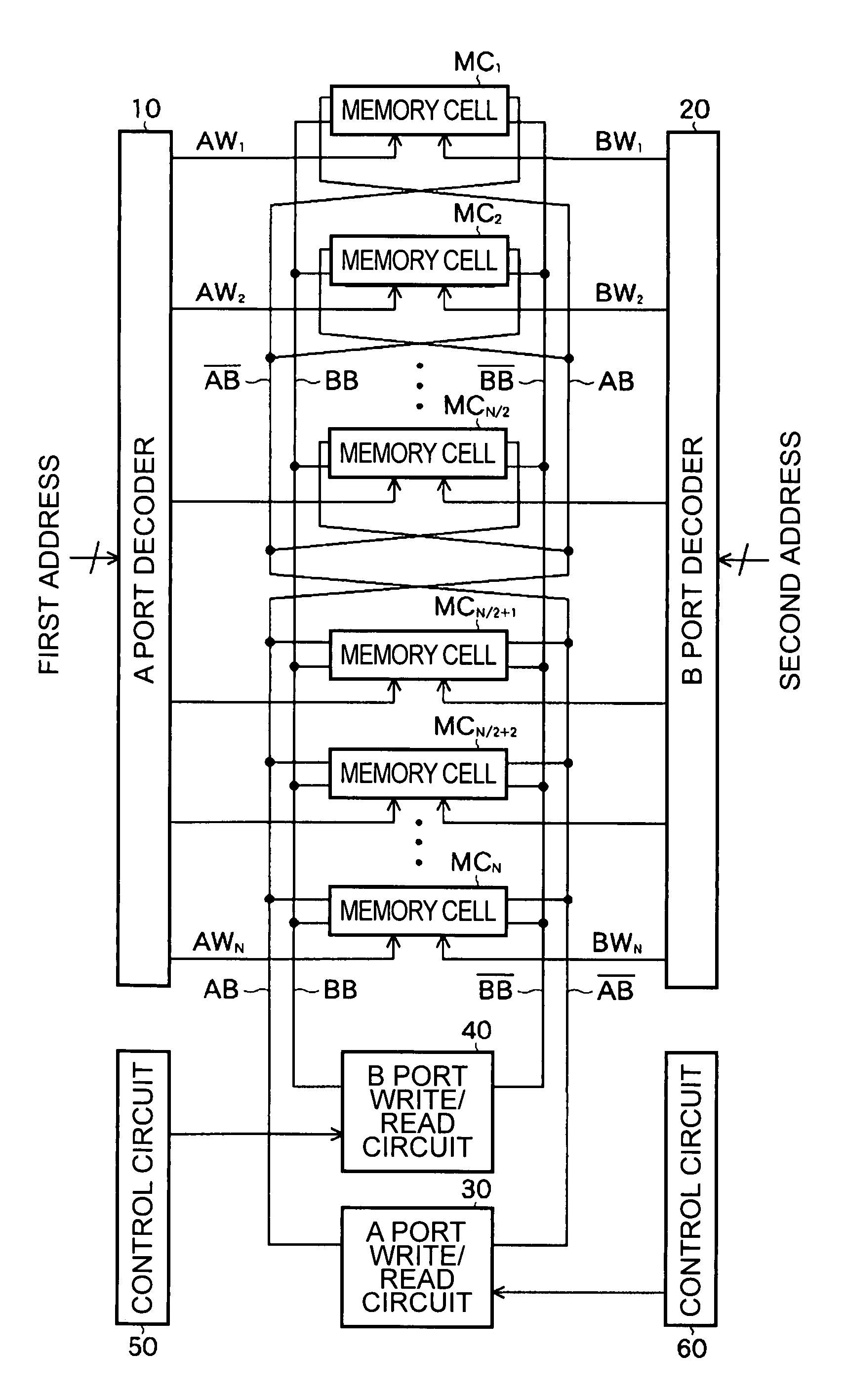
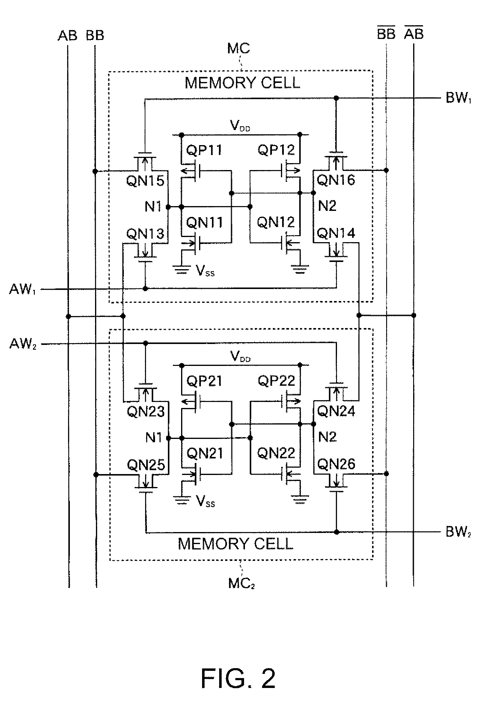
first embodiment
Bit line AB capacity: 401 fF
Bit line BB capacity: 461 fF
[0061]The specifications of the dual-port SRAM are determined by the port with the poorer characteristics, and thus, it is preferable that the bit line capacities of the two ports are balanced. The ratio of the bit line capacities of the two ports in the comparative example is 1.48. However, the ratio of the bit line capacities of the two ports according to the first embodiment is 1.15, and thus, it is clear that the imbalance between the capacities of the two ports have been improved.
[0062]Next, a second embodiment of the invention will be explained.
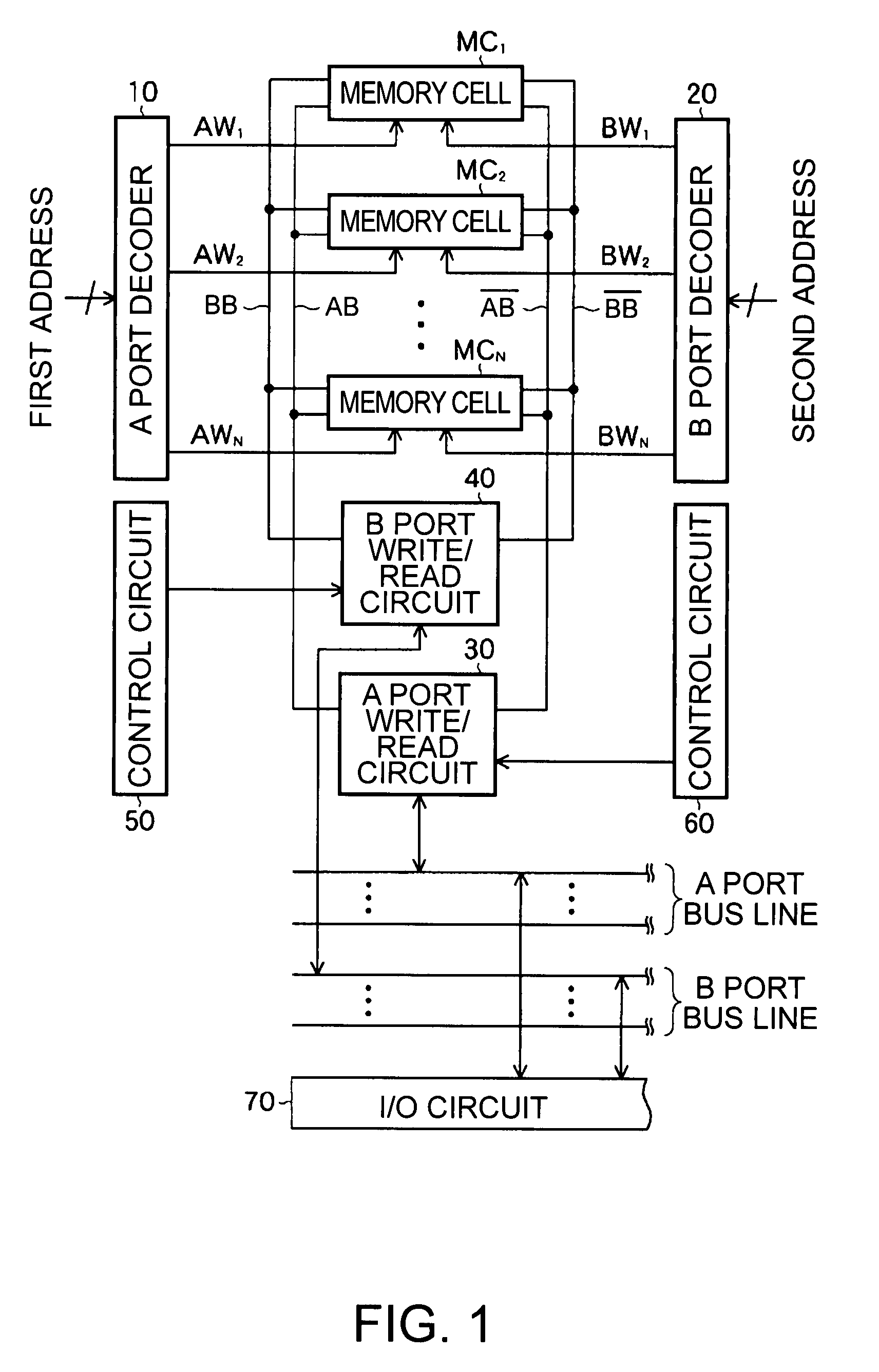
[0063]FIG. 5 is a block diagram showing a partial configuration of the dual port S1 embedded in the semiconductor integrated circuit according to the second embodiment of the invention. The dual-port SRAM differs from the dual-port SRAM according to the first embodiment, shown in FIG. 1, in layout only, and is the same as that in the first embodiment in other respects.
[0064]Accordi...
second embodiment
Bit line AB capacity: 433 fF
Bit line BB capacity: 461 fF
[0076]The specifications of the dual-port SRAM are determined by the port with the poorer characteristics, and thus, it is preferable that the bit line capacities of the two ports are balanced. The ratio of the bit line capacities of the two ports in the comparison example is 1.40. However, the ratio of the bit line capacities of the two ports according to the first embodiment is 1.06, and thus, it is clear that the imbalance between the capacities of the two ports is improved.
[0077]Designing of a semiconductor integrated circuit that has an internal dual-port SRAM is facilitated by the reduced difference in the characteristics between the two ports, and thus, designing period can be shortened. Furthermore, the operation timings of the two ports become closer due to the improvement in the imbalance in the timing at which the sense amplifier is turned on and the like, which determine the characteristics of data reading. As a res...
PUM
 Abstract
Description
Claims
Application Information