Surface mount poke-in connector

a surface mount and connector technology, applied in the direction of fixing connections, coupling device connections, contact members penetrating/cutting insulation/cable strands, etc., can solve the problems of time-consuming and costly steps of soldering wire leads to the boards, and achieve the effect of reducing the shadowing of the connector by the connector's low profil

Active Publication Date: 2008-11-11
TE CONNECTIVITY CORP
View PDF8 Cites 19 Cited by
  • Summary
  • Abstract
  • Description
  • Claims
  • Application Information

AI Technical Summary

Benefits of technology

[0009]This invention provides for a low profile feed-through surface mounted electrical connector (SMEC) for connecting at least two wire leads to a printed circuit board (PCB) or other suitable component surface. The low profile of the connector reduces shadowing by the connector when mounted on a PCB supporting LEDs. The SMEC is attached to the PCB by surface mount technology (SMT), a standardized automated process for placing and attaching electrical and electronic components to PCBs. Attachment may be by soldering, using a conductive adhesive, or other similar method.
[0022]In the exemplary embodiments, the housing may be formed of a high temperature material that is lightweight and high strength, and able to operate in a high temperature environment, such as along the surface of a PCB that supports LEDs. The housing may be formed of a high temperature liquid crystal polymer (LCP) such as Zenite 6330® by E.I. du Pont de Nemours and Company of Wilmington, Del. or a high temperature nylon such as Stanyl 46 HF® by DSM Engineering Plastics North America, Inc., based in Reading, Pa., or any other known industry acceptable non-conductive high temperature resin. The housing is designed with a low profile and small footprint so that it may be placed upon a PCB supporting lighting LEDs without shadowing or blocking the light emissions of the LEDs. The housing at least partially covers the contact.
[0024]The contact may be formed by first forming a predetermined shape from a conductive sheet and then forming the predetermined shape into a generally cylindrical geometry with extended attachment points. The first step in forming the contact is to stamp, cut or by other similar shaping methods form a predetermined shape from stock material. The stock material may be plated. Then, the predetermined shape is formed into the contact with extended attachment points by any material shaping method, including rolling and working. A combination of different shaping techniques may be used to complete the contact design. The extended attachment points of the contact may be provided with a beveled edge to assist in solder reflow during attachment to the PCB. Beveling the edge of the attachment points is important when pre-plated stock material is used to improve solder reflow.

Problems solved by technology

SMT allows for mounting electrical devices on both sides of a PCB, which was not possible using through hole mounting technology.
The step of soldering the wire leads to the boards is time consuming and costly.

Method used


Image

  • Surface mount poke-in connector
  • Surface mount poke-in connector
  • Surface mount poke-in connector

Examples


Embodiment Construction

[0039]The present invention now will be described more fully hereinafter with reference to the accompanying drawings in which preferred embodiments of the invention are shown. This invention may, however, be embodied in many different forms and should not be construed as limited to the embodiments set forth herein; rather, these embodiments are provided so that this disclosure will be thorough and complete and will fully convey the scope of the invention to those skilled in the art.

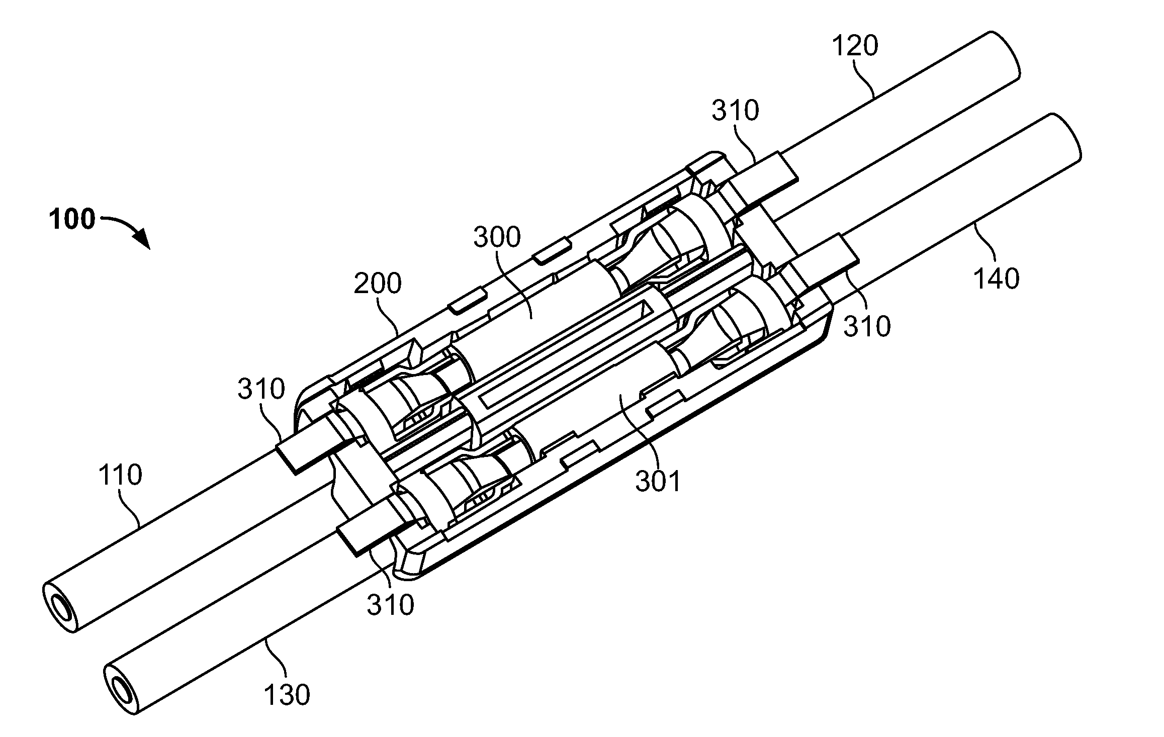
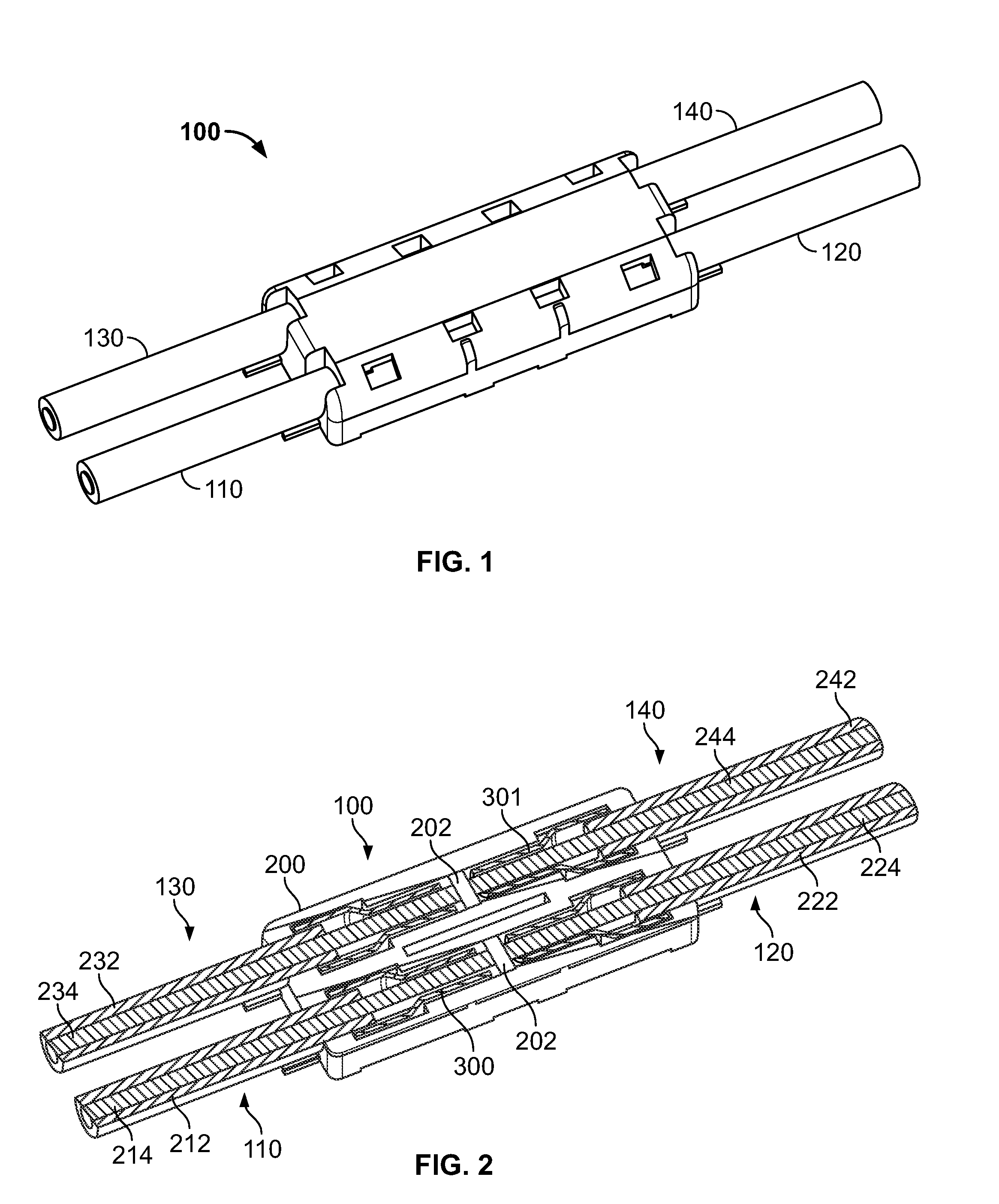
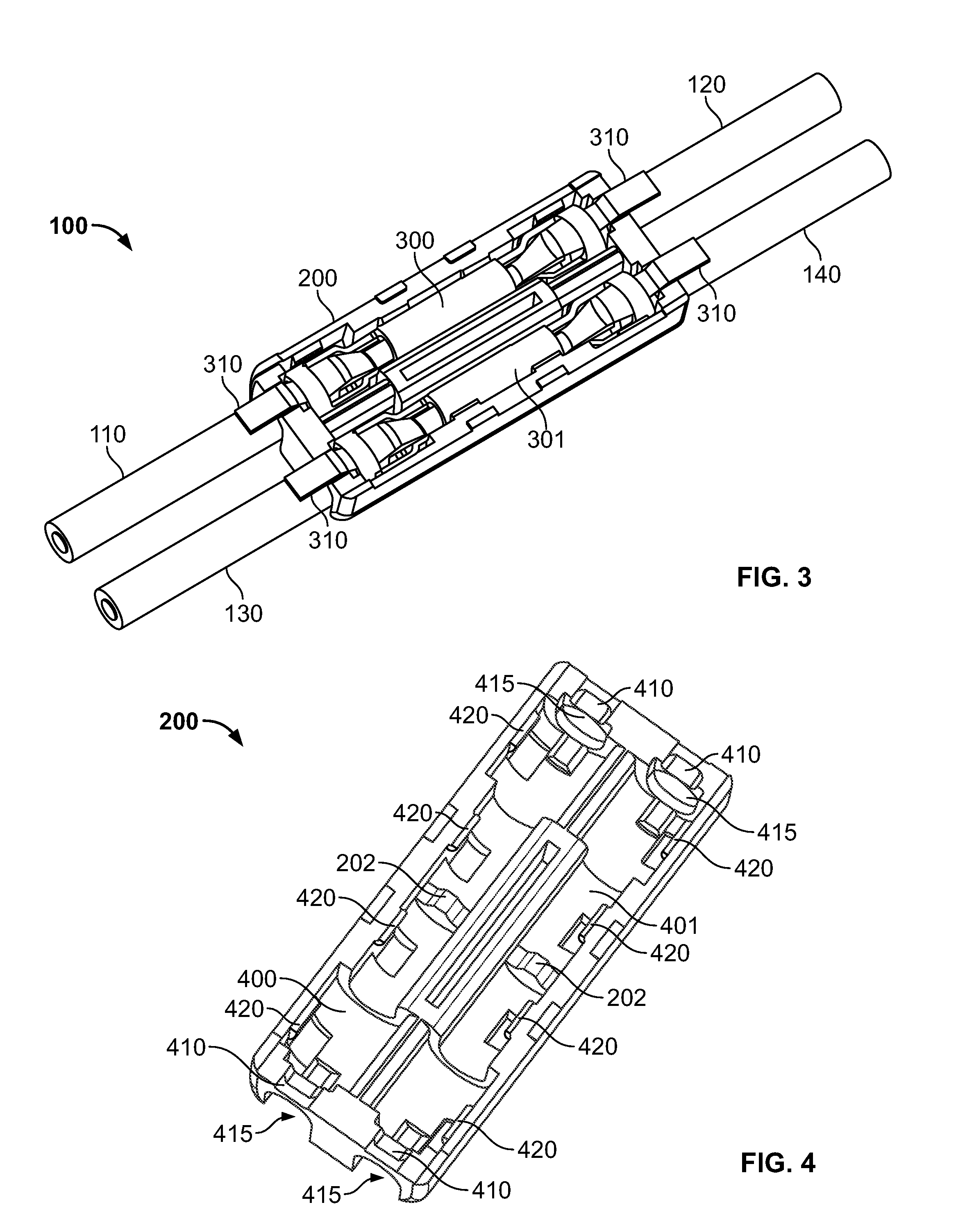
[0040]Referring to FIG. 1, an exemplary embodiment of the feed-through surface mount poke-in electrical connector 100 is depicted. The connector 100 provides a first electrical connection to a first pair of wires that includes a first wire 110 and second wire 120, and a second electrical connection to a second pair of wires that includes a third wire 130 and a fourth wire 140. The connector 100 may also connect the first wire 110 and the second wire 120 to an electrical trace (not shown) on an electrical ...


PUM


Abstract

A surface mount poke in connector is disclosed for mounting upon a surface of an electrical device such as printed circuit board, and is particularly applicable for printed circuit boards supporting LEDs. The connector includes a contact having an engaging mechanism for securing a first and second wire leads to the contact. The contact further has attachment points for connecting the connector to an electrical device surface by soldering.

Description

CROSS REFERENCE TO RELATED APPLICATIONS[0001]This application is a continuation-in-part, and claims the priority of U.S. non-provisional patent application No. 11 / 615,235 filed on Dec. 22, 2006, incorporated herein by reference in its entirety.FIELD OF THE INVENTION[0002]The present invention is directed to an electrical connector, and more specifically a feed-through surface mount electrical connector (SMEC) for connecting wire leads to an electrical device using surface mount technology (SMT). The electrical device may be a printed circuit board (PCB), but is not limited thereto. The PCB may contain light emitting diodes (LEDs). The invention is particularly well suited for connecting multiple PCBs in series.BACKGROUND OF THE INVENTION[0003]Electrical devices are often attached to printed circuit boards (PCBs) by soldering terminals of the electrical device to a surface of the PCB. Surface Mount Technology (SMT) is a particular method of soldering electrical terminals to a PCB. SM...

Claims


Application Information

Patent Timeline
Patent Type & Authority Patents(United States)
IPC IPC(8): H01R11/20
CPCH01R4/4818H01R9/2491H01R11/09H01R13/111H01R12/716H01R12/515H01R4/02H01R4/2404H01R12/58H01R13/03H01R13/422H01R43/0256H01R4/26H01R4/48185
Inventor WEBER, RONALD MARTINBUCHER, ALAN W.HORST, SHELDON LYNN
Owner TE CONNECTIVITY CORP
Why Eureka
Try Eureka