Supercharge Your Innovation With Domain-Expert AI Agents!

Buffer control circuit, semiconductor memory device for memory module including the buffer control circuit, and control method of the buffer control circuit

a buffer control circuit and memory module technology, applied in logic circuit coupling/interface arrangement, static indicating devices, instruments, etc., can solve the problems of increasing the difficulty of circuit designers increasing the difficulty of designing buffer control circuits, and increasing the difficulty of routing signal lines to transfer control signals doffb/b>1/b> from the control signal generator to the buffer control circuits. the effect of unnecessary power consumption

Active Publication Date: 2008-11-18
SK HYNIX INC
View PDF5 Cites 2 Cited by
  • Summary
  • Abstract
  • Description
  • Claims
  • Application Information

AI Technical Summary

Benefits of technology

This approach effectively reduces unnecessary power consumption by data input buffers during non-write periods, improving power management and facilitating easier signal routing in multi-device memory modules.

Problems solved by technology

When the data input buffer is enabled to perform the operation of receiving the external input data, current consumption of the semiconductor memory device rises abruptly.
However, in the event that the buffer control circuit 10 generates the buffer control signal ENDINDSB1 based on the control signal DOFFB1, a circuit designer may encounter lots of difficulties in designing the buffer control circuit 10.
As semiconductor chips are miniaturized due to the developments of semiconductor manufacturing technology, however, a designing work for routing a signal line that transfers the control signal DOFFB1 from the control signal generator to the buffer control circuit 10 becomes more difficult.
As a result, there is a problem in that the data input buffers INB1 to INBJ of the first semiconductor memory device consume power unnecessarily during the period T2.
There is also a problem in which the data input buffers INB1 to INBJ of each of the second to Uth semiconductor memory devices consume power unnecessarily during periods other than the read operation period of each of the second to Uth semiconductor memory devices.
This problem may become more profound when the number of semiconductor memory devices included in a memory module is increased.

Method used


Image

  • Buffer control circuit, semiconductor memory device for memory module including the buffer control circuit, and control method of the buffer control circuit
  • Buffer control circuit, semiconductor memory device for memory module including the buffer control circuit, and control method of the buffer control circuit
  • Buffer control circuit, semiconductor memory device for memory module including the buffer control circuit, and control method of the buffer control circuit

Examples


Embodiment Construction

[0035]The present invention will now be described in detail in connection with certain exemplary embodiments with reference to the accompanying drawings.

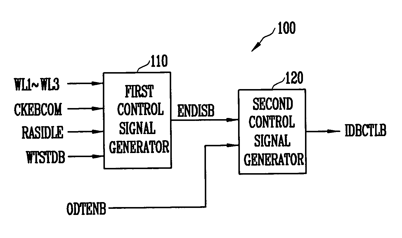
[0036]FIG. 3 is a block diagram of a buffer control circuit according to an embodiment of the present invention. Referring to FIG. 3, a buffer control circuit 100 includes a first control signal generator 110, and a second control signal generator 120.

[0037]The first control signal generator 110 generates an internal buffer control signal ENDISB in response to write latency signals WL1 to WL3 and internal control signals CKEBCOM, RASIDLE, and WTSTDB. The write latency signals WL1 to WL3 are respectively enabled or disabled according to write latency set in a semiconductor memory device (for example, SMD1) (refer to FIG. 6), which includes the buffer control circuit 100.

[0038]The term “write latency” refers to a time from which a write command is inputted to the semiconductor memory device SMD1 to when external input data IDQ1_1 to I...


PUM


Abstract

A buffer control circuit, a semiconductor memory device for a memory module including the buffer control circuit, and a control method of the buffer control circuit, in which power consumption can be reduced. The buffer control circuit includes a first control signal generator that generates an internal buffer control signal in response to write latency signals and internal control signals, and a second control signal generator that generates a buffer control signal in response to the internal buffer control signal and a termination control signal. It is therefore possible to reduce unnecessary power consumption incurred by a data input buffer.

Description

BACKGROUND[0001]1. Field of the Invention[0002]The present invention generally relates to a semiconductor memory device, and more particularly, to a buffer control circuit of a semiconductor memory device and control method thereof.[0003]2. Discussion of Related Art[0004]In general, a semiconductor memory device includes a data input buffer that receives data from an external device and outputs the externally input data to an internal core circuit including a memory cell array, during a write operation. When the data input buffer is enabled to perform the operation of receiving the external input data, current consumption of the semiconductor memory device rises abruptly. This is because the data input buffer receives the external input data through an external transmission line having a relatively high resistance value.[0005]To reduce current consumption by the data input buffer, it is very important to control the data input buffer to be disabled during the remaining periods excep...

Claims


Application Information

Patent Timeline
Patent Type & Authority Patents(United States)
IPC IPC(8): G11C7/00
CPCG11C7/1078G11C7/1084G11C7/109G11C7/1048G11C7/1051G11C7/22H03K19/017545H04L25/0278
Inventor KANG, SHIN DEOK
Owner SK HYNIX INC
Features
  • R&D
  • Intellectual Property
  • Life Sciences
  • Materials
  • Tech Scout
  • Unparalleled Data Quality
  • Higher Quality Content
  • 60% Fewer Hallucinations
Learn More