System and method of measuring and mapping three dimensional structures

a three-dimensional structure and surface technology, applied in the field of three-dimensional object measurement of the surface of three-dimensional objects, can solve the problems that the system cannot be directly applied to aspherical measurement and the surface irregularities of contact lens molds may be large,

Inactive Publication Date: 2008-11-25
AMO WAVEFRONT SCI
View PDF35 Cites 110 Cited by
  • Summary
  • Abstract
  • Description
  • Claims
  • Application Information

AI Technical Summary

Benefits of technology

[0005]There are a number of applications where the ability to provide a true measurement and map of a three-dimensional surface would be beneficial. There are also a number of applications where the ability to precisely and accurately determine characteristics (particularly one or more optical properties) of an optically transmissive device would be beneficial.
[0015]Accordingly, it would be advantageous to provide a system and method of measuring and mapping three-dimensional surfaces of spherical and aspherical objects. It would also be advantageous to provide such a system and method that operates with an improved dynamic range. Other and further objects and advantages will appear hereinafter.
[0017]In one aspect of the invention, a variable position optical system and a dynamic-range-limiting aperture are used, similar to that disclosed in the '917 patent, to ensure that a wavefront sensor operates always within its dynamic range. It is recognized that for an arbitrary optical device with strongly varying surface curvatures, it will not be possible to measure the entire element in a single operation (as it is for the ocular system using the system disclosed in the '917 patent). However, the inventors have recognized that, with different positions of the variable position optical system, it is possible to examine the entire surface of the element under test. Thus by systematically varying the position of the variable position optical system, it is possible to obtain measurements of the entire surface of the element under test, and then construct the measurement of a highly curved or aberrated element from these multiple individual measurements.

Problems solved by technology

Such contact lens molds may suffer not only from surface irregularities (small-scale features), but also may include large-area defects.
However, such a system cannot be directly applied to aspherical measurements of a contact lens mold, for example, because in most cases these elements are highly curved surfaces that cannot be probed with an injected beam system.
However, in many cases the requirements for dynamic range and / or accuracy exceed the ability of a particular measurement technology.
If the instrument is designed to meet a specific accuracy, then it will often have reduced dynamic range.
However, he carefully limits the application to rotationally symmetric systems so that the instrument can be operated within the dynamic range of the system.
Thus his device is of limited applicability to general aspherical shapes.
However, this does not solve the problem of spot overlap or gross aberration.
While these concepts are useful (in fact, one such method that has particular advantages is disclosed in detail below), they do not solve the problem of spot crossover when large changes in the wavefront gradient need to be measured.
It is recognized that for an arbitrary optical device with strongly varying surface curvatures, it will not be possible to measure the entire element in a single operation (as it is for the ocular system using the system disclosed in the '917 patent).

Method used


Image

  • System and method of measuring and mapping three dimensional structures
  • System and method of measuring and mapping three dimensional structures
  • System and method of measuring and mapping three dimensional structures

Examples


Embodiment Construction

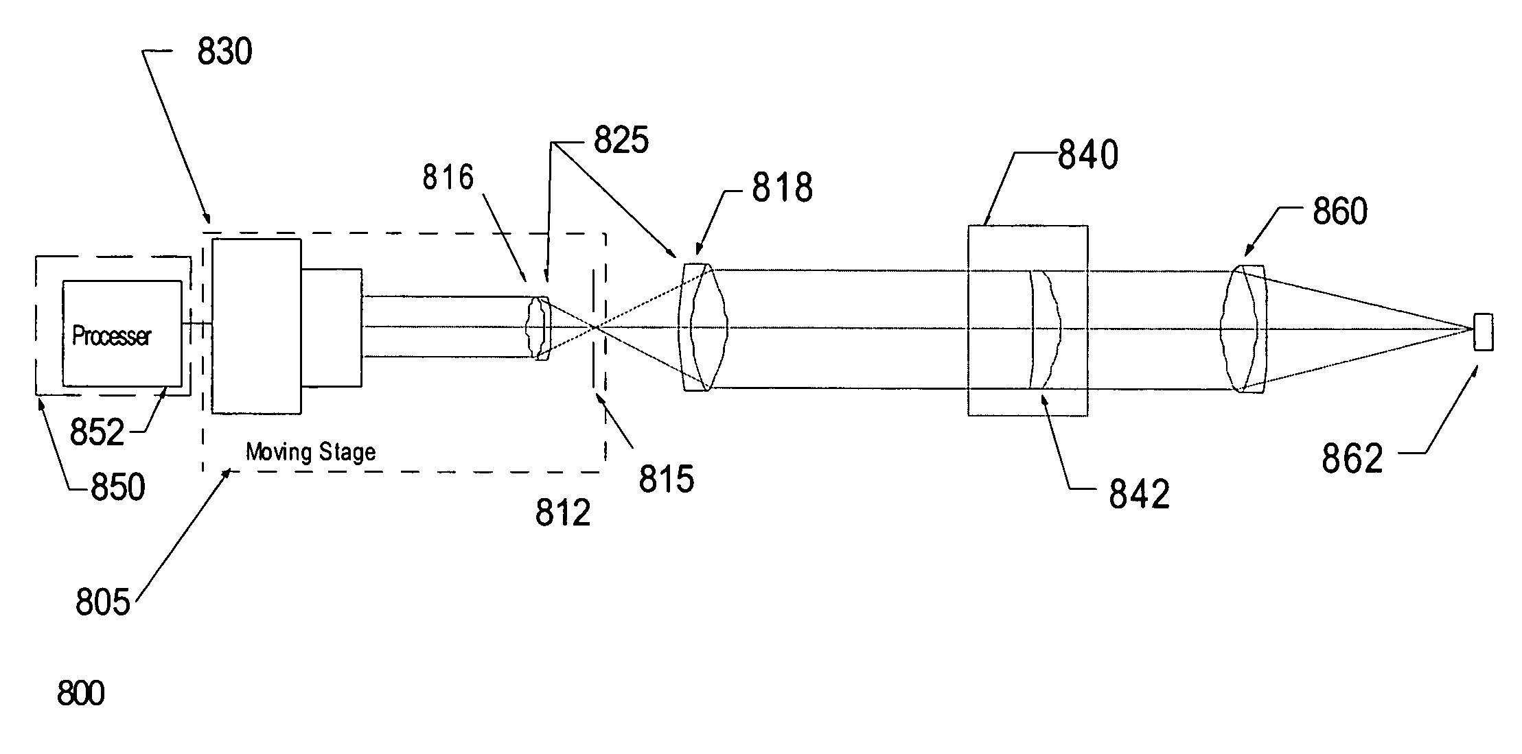
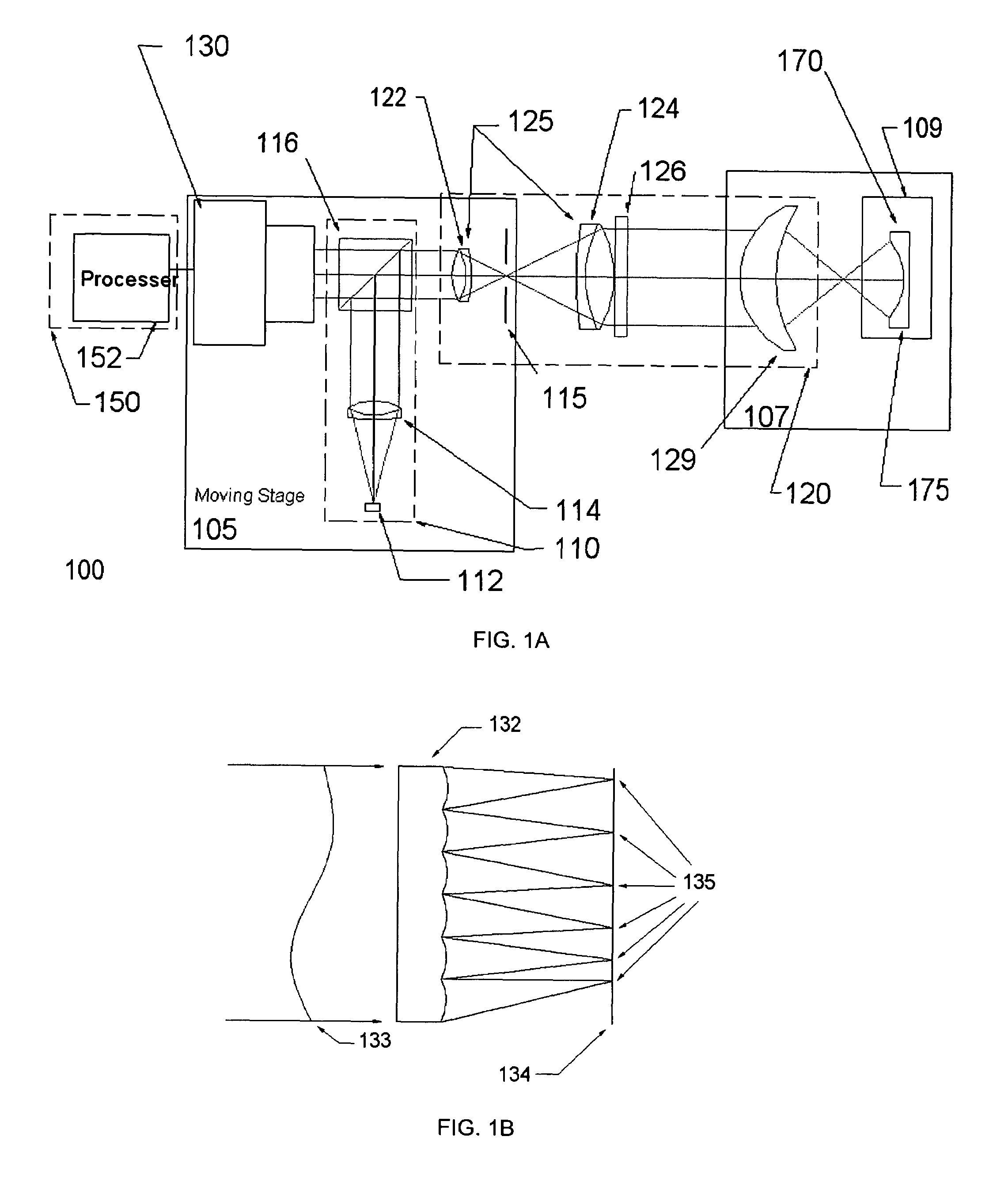
[0048]FIG. 1 shows a functional block diagram of one embodiment of a system 100 for measuring and mapping three-dimensional surfaces of spherical and aspherical objects.

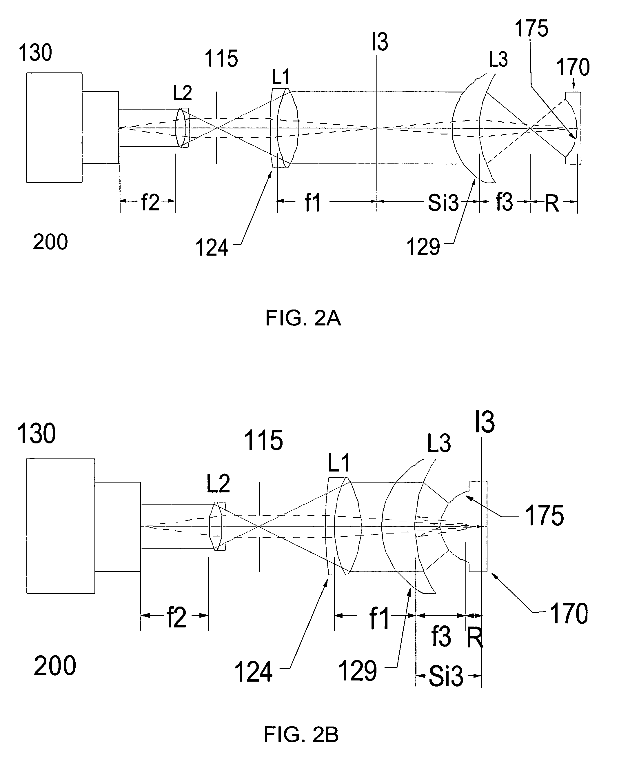
[0049]The system 100 includes: a projection system 110 comprising a light source 112, a collimating lens 114, and a polarizing beam splitter 116; an optical imaging system 120 comprising lens pair 122 and 124 (operating together as a telescope 125), dynamic-range-limiting aperture (RLA) 115, λ / 4 waveplate 126, and reformatting lens 129; a wavefront sensor 130; and a data analysis system 150 including a processor 152. Beneficially, the system also includes one or more movable stages—in particular the system 100 includes three movable stages 105, 107, and 109—on each of which one or more components may be mounted. The purposes and function of the movable stages will be explained in further detail below.

[0050]Beneficially, in one embodiment, the wavefront sensor 130 is a Shack-Hartmann wavefront sensor, an example of wh...


PUM


Abstract

A system for mapping a three-dimensional structure includes a projecting optical system adapted to project light onto an object, a correction system adapted to compensate the light for at least one aberration in the object, an imaging system adapted to collect light scattered by the object and a wavefront sensor adapted to receive the light collected by the imaging system and to sense a wavefront of the received light. For highly aberrated structures, a number of wavefront measurements are made which are valid over different portions of the structure, and the valid wavefront data is stitched together to yield a characterization of the total structure.

Description

CROSS-REFERENCES TO RELATED APPLICATIONS[0001]This application is a continuation-in-part of U.S. patent application Ser. No. 10 / 419,072, filed on 21 Apr. 2003 now abandoned which is in turn a continuation of U.S. patent application Ser. No. 09 / 692,483, filed on 20 Oct. 2000 and which issued on 22 Apr. 2003 as U.S. Pat. No. 6,550,917, which application in turn claims priority under 35 U.S.C. § 119 from U.S. Provisional Patent Application No. 60 / 182,088 filed on 11 Feb. 2000, the entire contents of each of which applications are hereby incorporated by reference in their entirety for all purposes as if fully set forth herein. This application is also a continuation-in-part of U.S. patent application Ser. No. 10 / 369,513, filed on 21 Feb. 2003, now U.S. Pat. No. 6,908,196, the entire contents of which are hereby incorporated by reference in their entirety for all purposes as if fully set forth herein.BACKGROUND AND SUMMARY[0002]1. Field[0003]This invention pertains to the field of measur...

Claims


Application Information

Patent Timeline
Patent Type & Authority Patents(United States)
IPC IPC(8): A61B3/10A61B3/103A61B3/11A61B3/113A61B3/12A61B3/15
CPCG01B11/306G01J9/00G01M11/0257
Inventor NEAL, DANIEL R.COPLAND, RICHARD JAMESNEAL, DAVID A.
Owner AMO WAVEFRONT SCI
Why Eureka
Try Eureka