Resist material and pattern formation method using the same

a technology of resist material and pattern, applied in the direction of photosensitive materials, instruments, photomechanical equipment, etc., can solve the problems of reducing the productivity and yield in the fabrication process of semiconductor devices, degrading the shape, etc., and achieve the effects of increasing dissolution contrast, and suppressing surface roughness and pattern roughness

Inactive Publication Date: 2008-11-25
PANASONIC CORP
View PDF5 Cites 4 Cited by
  • Summary
  • Abstract
  • Description
  • Claims
  • Application Information

AI Technical Summary

Benefits of technology

[0022]On the other hand, in an unexposed portion, the solubility of the non-substituted sulfonamide of the remaining part is inhibited by the part of the vinyl sulfonamide substituted with an acetal group, and hence, the dissolution contrast is increased. This high dissolution contrast attained by the smooth dissolution of the exposed portion and the insolubility of the unexposed portion can effectively suppress the surface roughness and the pattern roughness.
[0023]Furthermore, since a unit of the polymeric material used for forming the resist film is shared by the substituted and non-substituted sulfonamides, the exposed portion is uniformly dissolved, and this also suppresses the surface roughness and the pattern roughness. It is noted that a non-substituted sulfonamide group exhibits an effect to improve the adhesion of the pattern owing to its polarity.
[0026]The polymeric material included in the resist material of this invention can be fabricated by obtaining a polymer through polymerization of vinyl sulfonamide, that is, a monomer, and allowing an acetal group, that is, an acid labile group, to react with the polymer. In this fabrication method, the substitution ratio of the acetal group can be easily controlled to a desired ratio. Needless to say, the present invention is not limited to this fabrication method.
[0028]The resist material of this invention may further include a dissolution inhibitor for inhibiting dissolution of the polymeric material. The dissolution inhibitor improves the dissolution contrast between an unexposed portion and an exposed portion of a resist film. An example of the dissolution inhibitor is bis-t-butyloxycarbonylated bisphenol A, which does not limit the invention. The ratio of the dissolution inhibitor to the polymeric material is preferably approximately 1 wt % through 10 wt %.
[0030]In the first pattern formation method, the resist material of this invention is used for forming a resist pattern in a good shape free from surface roughness and pattern roughness.
[0033]In the second pattern formation method, the pattern exposure is carried out with the liquid provided on the resist film, namely, through what is called immersion lithography, differently from the first pattern formation method. Also in the case where the immersion lithography is employed, a resist pattern can be formed in a good shape free from the surface roughness and the pattern roughness by using the resist material of this invention. In the immersion lithography, a region in an exposure system sandwiched between a projection lens and a resist film formed on a wafer is filled with a liquid having a refractive index larger than that of air, and therefore, the NA (the numerical aperture of the projection lens) of the exposure system can be theoretically increased to the refractive index of the liquid maximally. As a result, the resolution of the resist film can be improved. Furthermore, the depth of focus can be also increased in the immersion lithography.

Problems solved by technology

In the resist pattern 2a obtained by the pattern formation method using the conventional resist material, however, surface roughness and pattern roughness are frequently caused, resulting in degrading its shape (see, for example, G. Lee et al., Proc.
When a resist pattern in such a degraded shape is used in etching, a pattern obtained in the etched film is also in a degraded shape, and hence, the productivity and the yield in the fabrication process for semiconductor devices are disadvantageously lowered.

Method used


Image

  • Resist material and pattern formation method using the same
  • Resist material and pattern formation method using the same
  • Resist material and pattern formation method using the same

Examples


embodiment 1

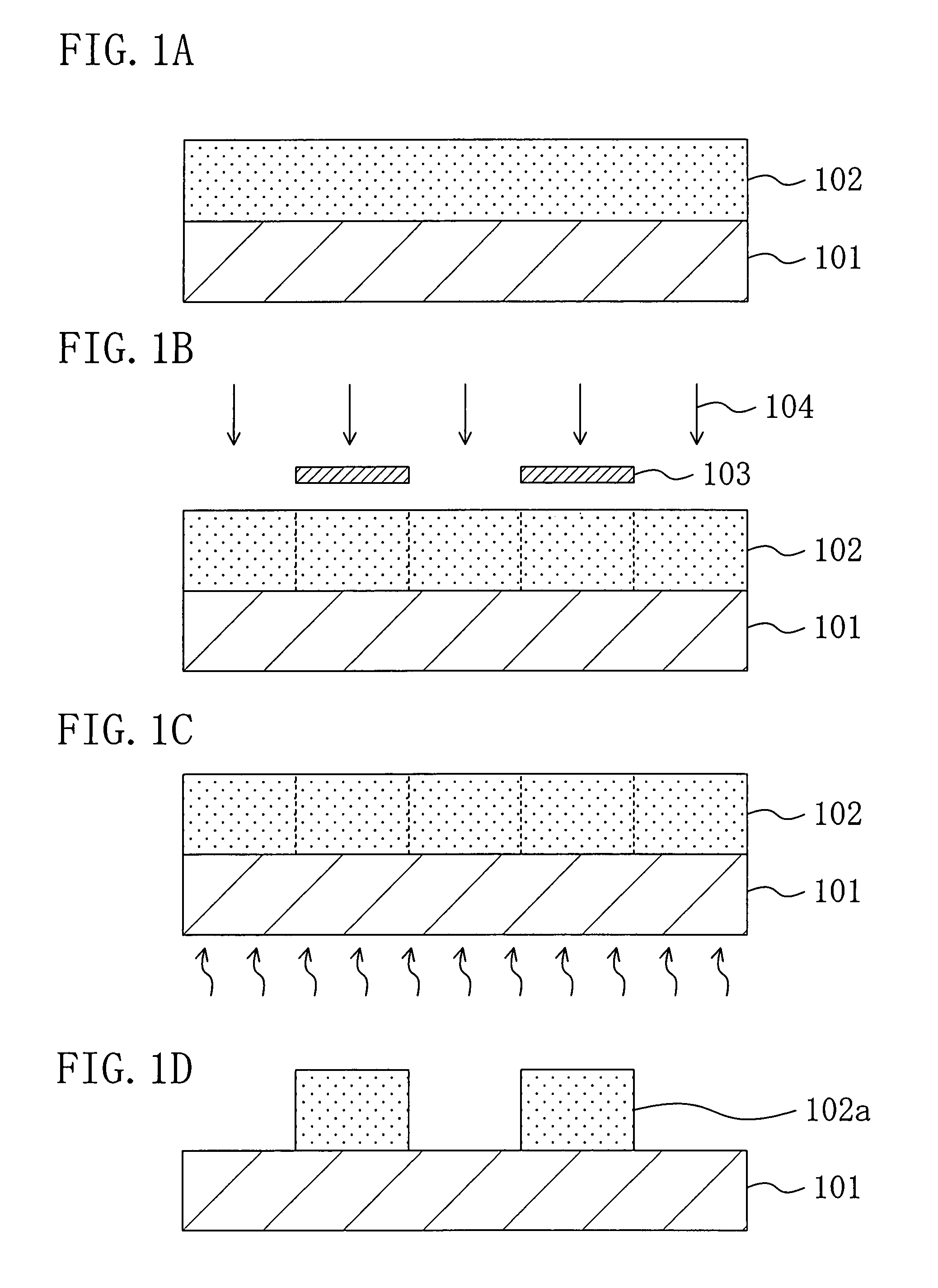
[0042]A pattern formation method according to Embodiment 1 of the invention will now be described with reference to FIGS. 1A through 1D.

[0043]First, a positive chemically amplified resist material having the following composition is prepared:

[0044]Base polymer: poly(vinyl di(adamantoxymethylsulfonamide) (30 mol %)-vinyl sulfonamide (70 mol %)) . . . 2 g.

[0045]Acid generator: triphenylsulfonium trifluoromethane sulfonate . . . 0.06 g.

[0046]Quencher: triethanolamine . . . 0.002 g.

[0047]Solvent: propylene glycol monomethyl ether acetate . . . 20 g

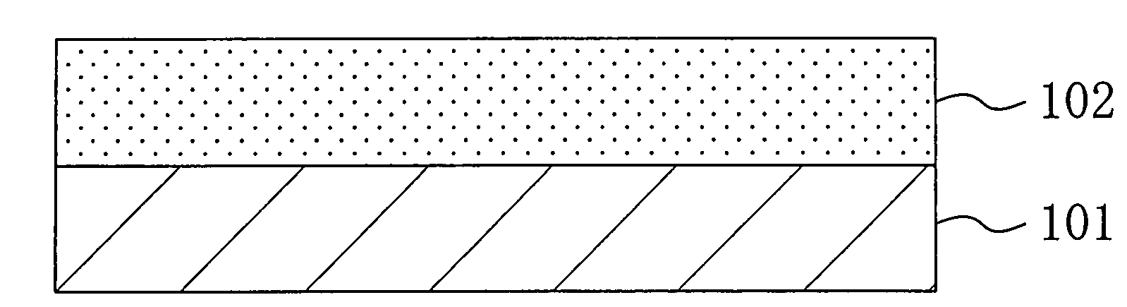
[0048]Next, as shown in FIG. 1A, the chemically amplified resist material is applied on a substrate 101, so as to form a resist film 102 with a thickness of 0.35 μm.

[0049]Then, as shown in FIG. 1B, the resist film 102 is subjected to pattern exposure by irradiating with exposing light 104 of ArF excimer laser having NA of 0.85 through a mask 103.

[0050]After the pattern exposure, as shown in FIG. 1C, the resist film 102 is baked by using a hot ...

embodiment 2

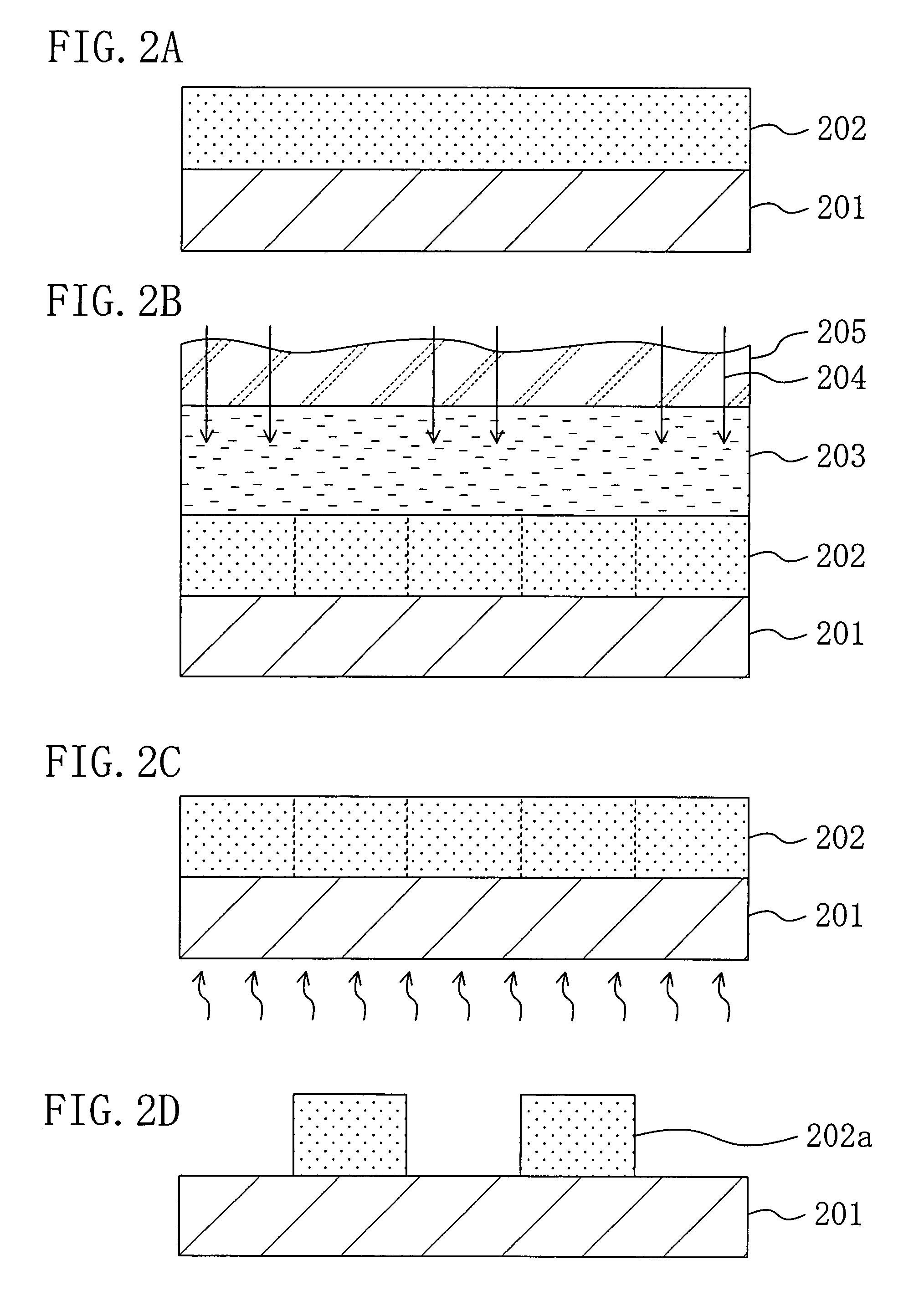
[0057]A pattern formation method according to Embodiment 2 of the invention will now be described with reference to FIGS. 2A through 2D.

[0058]First, a positive chemically amplified resist material having the following composition is prepared:

[0059]Base polymer: poly(vinyl di(adamantoxymethylsulfonamide) (30 mol %)-vinyl adamantoxymethylsulfonamide (5 mol %)-vinyl sulfonamide (65 mol %)) . . . 2 g.

[0060]Acid generator: triphenylsulfonium trifluoromethane sulfonate . . . 0.06 g.

[0061]Quencher: triethanolamine . . . 0.002 g.

[0062]Solvent: propylene glycol monomethyl ether acetate . . . 20 g.

[0063]Next, as shown in FIG. 2A, the chemically amplified resist material is applied on a substrate 201, so as to form a resist film 202 with a thickness of 0.35 μm.

[0064]Then, as shown in FIG. 2B, an immersion liquid 203 of water is provided between the resist film 202 and a projection lens 205. Under these conditions, the resist film 202 is subjected to pattern exposure by irradiating with exposin...


PUM

PropertyMeasurementUnit
carbon numberaaaaaaaaaa
wavelengthaaaaaaaaaa

Abstract

A resist material includes a polymeric material made of a unit represented by a general formula of the following Chemical Formula; and an acid generator for generating an acid through irradiation with light:wherein R1, R2 and R3 are the same or different and are a hydrogen atom, a fluorine atom, or a straight-chain alkyl group, a branched or cyclic alkyl group or a fluoridated alkyl group with a carbon number not less than 1 and not more than 20; R is a hydrogen atom, a straight-chain alkyl group, a branched or cyclic alkyl group or a fluoridated alkyl group with a carbon number not less than 1 and not more than 20; m≧0, n≧0, s>0 (whereas excluding m=n=0) and 1≦k≦3.

Description

CROSS-REFERENCE TO RELATED APPLICATIONS[0001]This application claims priority under 35 U.S.C. §119 on Patent Application No. 2006-118035 filed in Japan on Apr. 21, 2006, the entire contents of which are hereby incorporated by reference.BACKGROUND OF THE INVENTION[0002]The present invention relates to a resist material suitably used in microprocessing technique for semiconductor devices and a pattern formation method using the same.[0003]Recently, in accordance with the increased degree of integration and the increased operation speed of LSIs, a pattern rule is required to be further refined. The pattern rule has been rapidly refined owing to the increased NA (numerical aperture) of a projection lens, the improved performance of a resist material, the reduced wavelength of exposing light and the like.[0004]Currently, ArF excimer laser (of a wavelength of a 193 nm band) is used as the exposing light for coping with a design rule of 90 nm or less.[0005]Now, a pattern formation method u...

Claims


Application Information

Patent Timeline
Patent Type & Authority Patents(United States)
IPC IPC(8): G03F7/00G03F7/004C08F220/38G03F7/039H01L21/027
CPCC08F259/00C08F291/00G03F7/0392
Inventor ENDO, MASAYUKISASAGO, MASARU
Owner PANASONIC CORP
Why Eureka
Try Eureka