Image pickup device

Inactive Publication Date: 2008-11-25
CANON KK
View PDF20 Cites 20 Cited by
  • Summary
  • Abstract
  • Description
  • Claims
  • Application Information

AI Technical Summary

Benefits of technology

[0010]It is an object of the invention to reduce fixed pattern noises (FPN) caused by variation in residual image characteristics of soli

Problems solved by technology

It is therefore difficult to form a sufficient potential gradient between the photodiode and charge accumulation region when the signal charges are transferred.
Pixels unable to realize a suffic

Method used


Image

  • Image pickup device
  • Image pickup device
  • Image pickup device

Examples


second embodiment

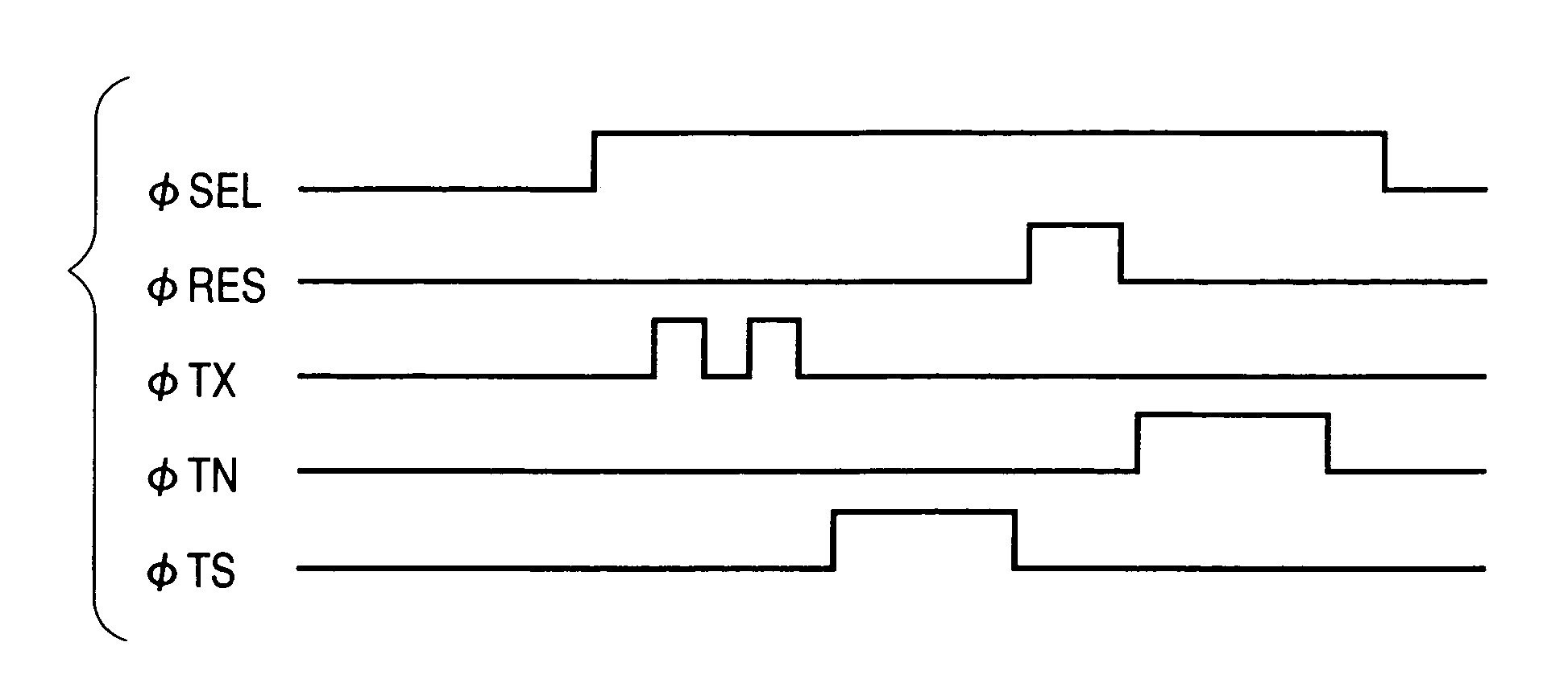
[0028]In the invention, a solid state image pickup device shown in FIG. 5 is driven by drive pulses shown in FIG. 6.

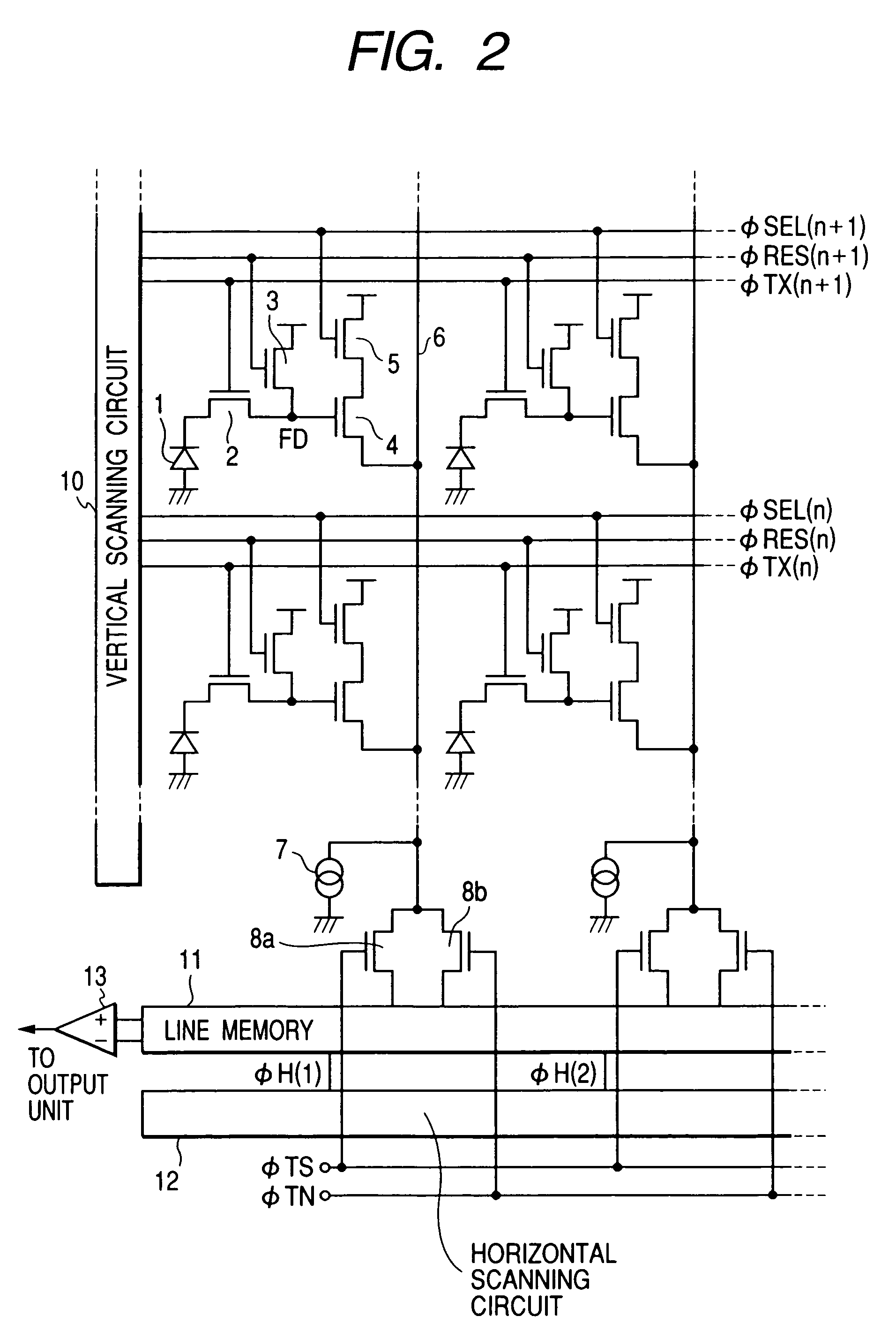
[0029]Referring to FIG. 5, each pixel has a photodiode 1, a transfer switch 2, a reset switch 3, a pixel amplifier 4 and a row select switch 5. The second embodiment is different from the first embodiment in that the row select switch 5 is provided on the side of a vertical output line 6 to which photoelectric conversion charges are output from the pixel amplifier 4.

[0030]In the circuit shown in FIG. 5, when the row select switch 5 is turned on upon reception of the select pulse φSEL, a source follower circuit constituted of a load current source 7 and the pixel amplifier 4 becomes active, so that outputs of the selected row are transferred to a vertical output line 6 and stored via transfer gates 8a and 8b into a line memory 11. The outputs temporarily stored in the line memory 11 are sequentially read out to an output unit under the control of a horizontal scanning c...

first embodiment

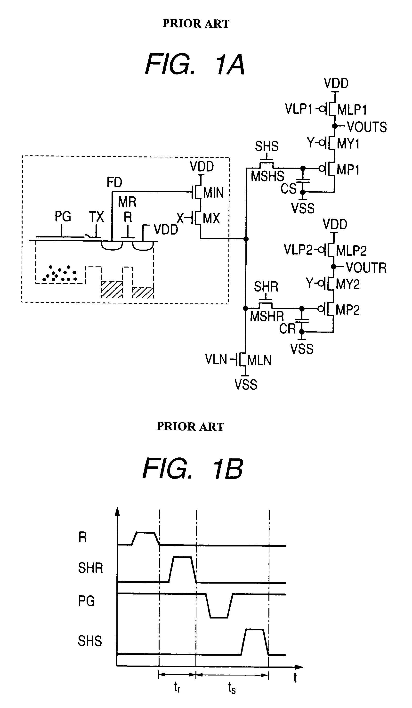
[0034]In this embodiment, the order of reading the photoelectric conversion charge output and reset output is reversed from that of the first embodiment in order to calculate a difference between correlated signals and reduce the reset output noises. In a moving picture output operation of a solid state image pickup device using a method of reading correlated signals as in this embodiment, a period of transferring signal charges by applying a transfer pulse is generally in the order of several microseconds. However, with the driving method of the present invention, charges can be transferred quickly in a limited transfer period.

[0035]The falling edge of the transfer pulse φTX is slanted to prevent charges from being returned to the photodiode when the transfer switch is turned off. Accordingly, in this embodiment, a photoelectric conversion charge signal of good noise characteristics from which not only fixed pattern noises but also random noises are reduced, can be obtained.

[0036]A...


PUM


Abstract

An image pickup device includes pixels each including a photoelectric conversion unit and a transfer switch for transferring a photoelectric conversion signal generated by the photoelectric conversion unit, and a driver for applying a pulse to the transfer switch a plurality of times when the signal generated by the photoelectric conversion unit is transferred via the transfer switch.

Description

BACKGROUND OF THE INVENTION[0001]1. Field of the Invention[0002]The present invention relates to an image pickup device and drive method thereof.[0003]2. Related Background Art[0004]Research and development of an image sensor called a CMOS type image sensor which reads out a photoelectric conversion signal not with a CCD (charge coupled device) but with a MOS transistor, are becoming active nowadays.[0005]This CMOS type image sensor is expected as an image sensor particularly for portable application because a CMOS logic LSI process can be used to fabricate the image sensor of such the type, a peripheral circuit can be integrated on a chip, and the CMOS type image sensor can be driven at a low voltage with a low power consumption. If a CMOS type image sensor is applied to technical fields requesting a high image quality, such as digital camera image pickup elements, it is necessary to provide some countermeasures against fixed pattern noises and random noises in order to obtain an i...

Claims


Application Information

Patent Timeline
IPC IPC(8): H04N3/14H04N5/335H01L27/146H04N5/341H04N5/355H04N5/363H04N5/365H04N5/374H04N5/3745
CPCH01L27/14643H04N3/1568H04N5/3597H04N25/626
Inventor HIYAMA, HIROKISUGAWA, SHIGETOSHIUENO, ISAMUKOIZUMI, TORUKOCHI, TETSUNOBUSAKURAI, KATSUHITOYAMASHITA, YUICHIROYONEDA, TOMOYA
Owner CANON KK
Why Eureka
Try Eureka