
Quantum well lasers with strained quantum wells and dilute nitride barriers

a quantum well and laser technology, applied in the field of quantum well lasers with strained quantum wells and dilute nitride barriers, can solve the problems of poor lasing performance of early ingaasn qw lasers, poor lasing performance of 1300 nm inp-based diode lasers at high-temperature operation, and poor quality of semiconductor crystals

Active Publication Date: 2008-11-25
WISCONSIN ALUMNI RES FOUND
View PDF66 Cites 28 Cited by
  • Summary
  • Abstract
  • Description
  • Claims
  • Application Information

AI Technical Summary

Benefits of technology

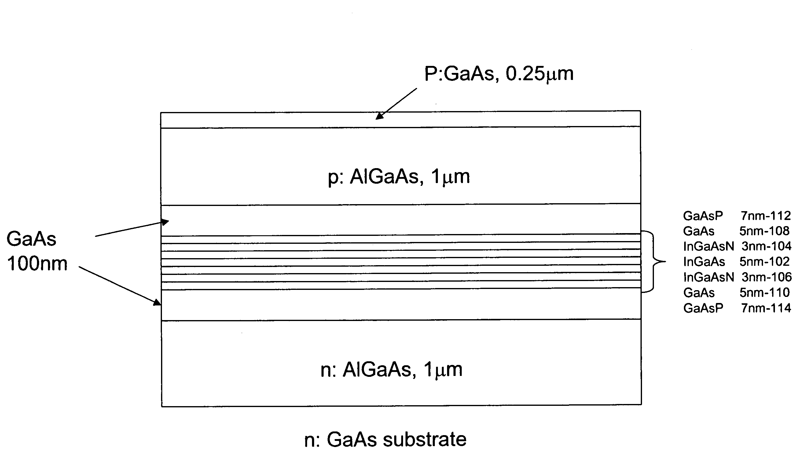
The present invention relates to optoelectronic devices made of GaAs-based semiconductors that can generate light at long wavelengths, such as 1.3 μm or higher. The devices have an active region with a well layer composed of a compressively-strained semiconductor that is free of nitrogen, which is placed between two barrier layers composed of a nitrogen- and indium-containing semiconductor. The optoelectronic devices can be used in amplifiers, light emitting diodes, and lasers. The invention provides a way to increase the optical gain of the devices by using multiple well layers and nitrogen-containing barrier layers. The semiconductor layers can be epitaxially deposited on a substrate of GaAs using conventional deposition techniques.

Problems solved by technology

Unfortunately, these 1300 nm InP-based diode lasers suffer poor lasing performance at high-temperature operation.
Unfortunately, early InGaAsN QW lasers suffer from poor lasing performance due to the utilization of nearly lattice-matched InGaAsN.
Unfortunately, the use of nitrogen in the quantum wells of the InGaAsN QW lasers decreases the quality of the semiconductor crystal, increasing the risk of device failure.

Method used


Image

  • Quantum well lasers with strained quantum wells and dilute nitride barriers
  • Quantum well lasers with strained quantum wells and dilute nitride barriers
  • Quantum well lasers with strained quantum wells and dilute nitride barriers

Examples


Embodiment Construction

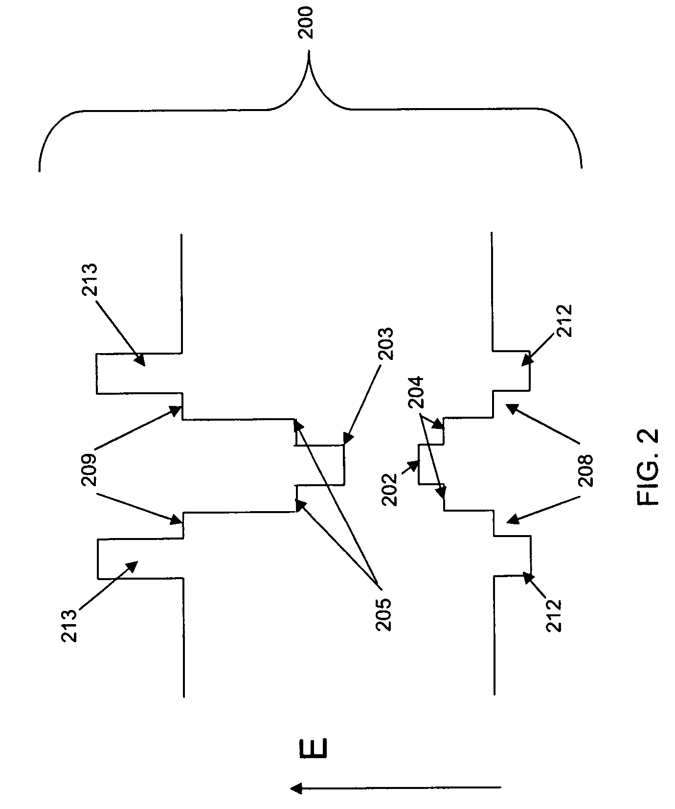
[0023]The present invention provides high-performance optoelectronic devices with an emission wavelength of 1200 nm, or higher, utilizing nitrogen-free (or substantially nitrogen-free) well layers with dilute nitride barrier layers. Tensile-strained barrier layers disposed beyond the dilute nitride barrier layers are desirably included to provide strain compensation to the compressively-strained InGaAs quantum wells. Spacer layers may separate the tensile-strained barrier layers from the dilute nitride barrier layers. These spacer layers may be used to achieve longer wavelength emission and / or to suppress diffusion between the tensile-strained barrier layers and the dilute nitride barrier layers.

[0024]For the purposes of this disclosure a well layer is “substantially free of nitrogen” as long as any nitrogen present in the layer is due only to diffusion between the well layer and a neighboring semiconductor layer. Thus, the term “substantially free of nitrogen” is intended to accoun...


PUM


Abstract

In accordance with the present invention, GaAs-based optoelectronic devices have an active region that includes a well layer composed of a compressively-strained semiconductor that is free, or substantially free, of nitrogen disposed between two barrier layers composed of a nitrogen- and indium-containing semiconductor.

Description

STATEMENT OF GOVERNMENT RIGHTS[0001]This invention was made with United States Government support awarded by the following agencies: Department of Defense ARPA under grant number DAAD19-03-1-0367, and National Science Foundation under grant number NSF 0355442. The United States has certain rights in this invention.FIELD OF THE INVENTION[0002]The present invention relates generally to the field of GaAs-based optoelectronic devices such as light emitting diodes and semiconductor diode lasers incorporating highly strained quantum wells with dilute nitride barriers.BACKGROUND OF THE INVENTION[0003]Conventional 1300 nm lasers are based on the InGaAsP or InGaAlAs quantum-well (QW) active material system on an InP substrate. Unfortunately, these 1300 nm InP-based diode lasers suffer poor lasing performance at high-temperature operation. (See, Belenky et al, IEEE J. Quantum Electron, vol. 35, pp. 1515, 1999.) The InGaAsN material system has also been introduced as a material system with eno...

Claims


Application Information

Patent Timeline
Patent Type & Authority Patents(United States)
IPC IPC(8): H01S3/04H01S5/12
CPCB82Y20/00H01S5/34313H01L33/06H01L33/30H01L33/32H01S5/028H01S5/12H01S5/18311H01S5/2009H01S5/2206H01S5/2231H01S5/3211H01S5/32366H01S5/3406H01S5/3422
Inventor MAWST, LUKE J.TANSU, NELSONYEH, JENG-YA
Owner WISCONSIN ALUMNI RES FOUND
Learn More