Wafer bonding method

a technology of wafer bonding and silicon, applied in the direction of contact members penetrating/cutting insulation/cable strands, radiation controlled devices, transistors, etc., can solve the problem of large chip area consumed by lateral oriented devices, more complex and expensive to fabricate a computer chip with memory embedded in this way, and the masks used to fabricate memory devices are not compatible with the masks used. problem, to achieve the effect of reducing the number of defects

Active Publication Date: 2008-12-30
BESANG
View PDF12 Cites 253 Cited by
  • Summary
  • Abstract
  • Description
  • Claims
  • Application Information

AI Technical Summary

Benefits of technology

[0012]The present invention provides a method of coupling substrates together which includes providing a first substrate; providing a second substrate with a conductive bonding region coupled to it; providing heat to the conductive bonding region to reduce its number of defects; and bonding the surface of the conductive bonding region to the first substrate so that the conductive bonding region and the first substrate are coupled together.

Problems solved by technology

However, these laterally oriented devices consume significant amounts of chip area.
However, there are several problems with doing this.
One problem is that the masks used to fabricate the memory devices are not compatible with the masks used to fabricate the other devices on the computer chip.
Hence, it is more complex and expensive to fabricate a computer chip with memory embedded in this way.
Another problem is that memory devices tend to be large and occupy a significant amount of area.
Further, the yield of the computer chips fabricated in a run decreases as their area increases, which increases the overall cost.
There are several problems, however, with using 3-D packages and 3-D ICs.
One problem is that the use of wire bonds increases the access time between the computer and memory chips because the impedance of wire bonds and large contact pads is high.
Similarly, the contact pads in 3-D ICs have correspondingly large capacitances which also increase the access time between the processor and memory circuits.
Another problem with using 3-D packages and 3-D ICs is cost.
The use of wire bonds is expensive because it is difficult to attach them between the processor and memory circuits and requires expensive equipment.
Further, it requires expensive equipment to align the various devices in the 3-D IC.
The bonding and alignment is made even more difficult and expensive because of the trend to scale devices to smaller dimensions.

Method used


Image

  • Wafer bonding method
  • Wafer bonding method
  • Wafer bonding method

Examples


Embodiment Construction

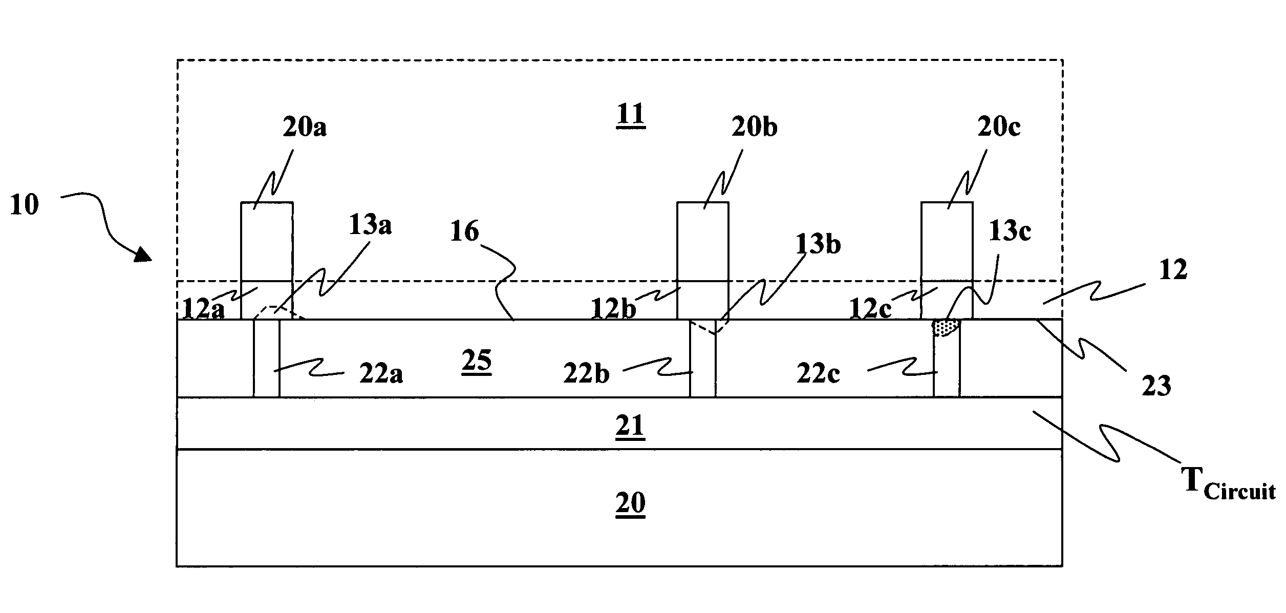
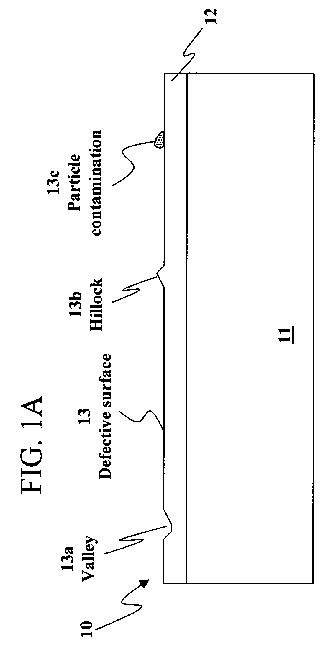
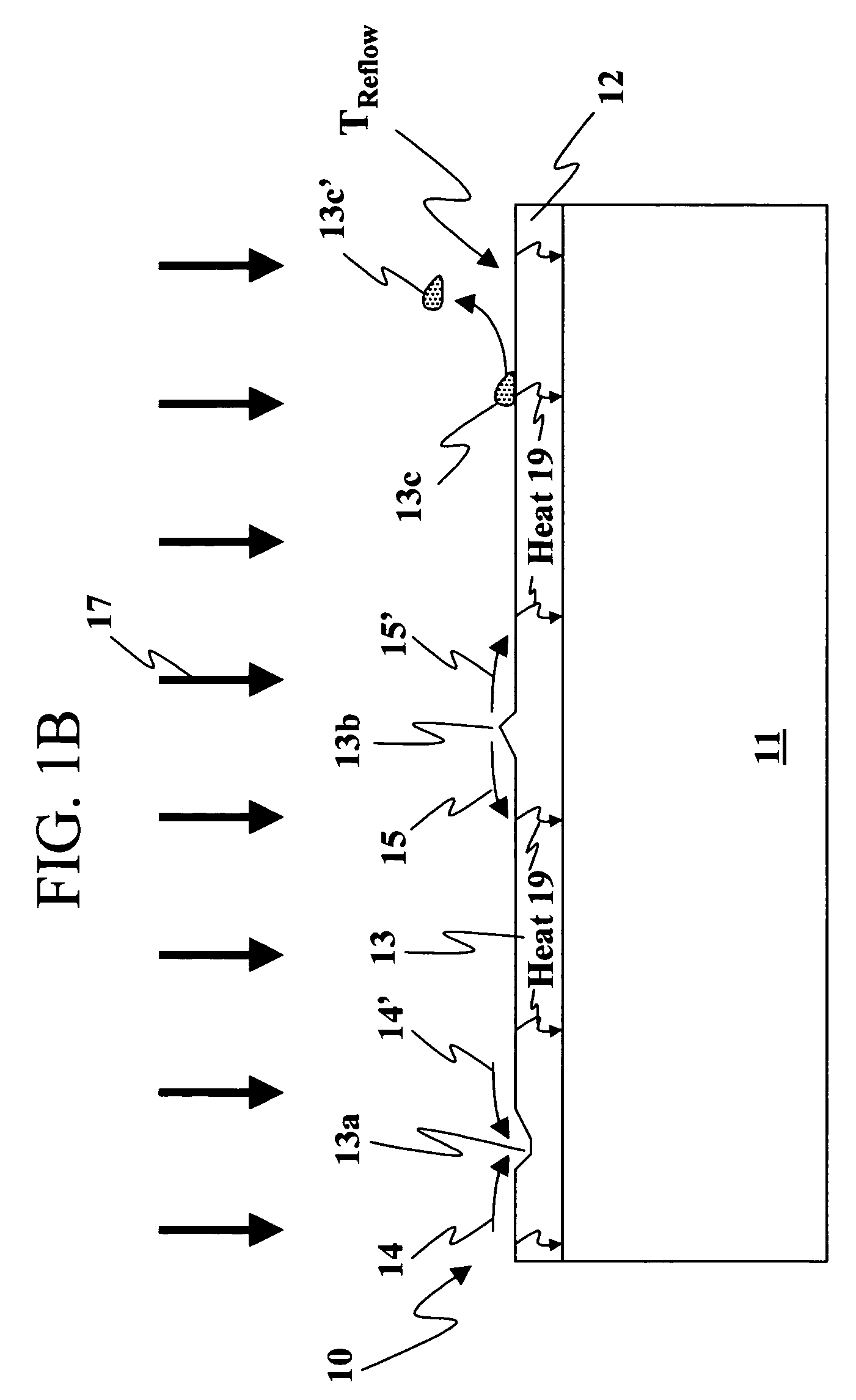
[0019]FIGS. 1A-1F are simplified sectional views of steps in fabricating a circuit 10 in accordance with the present invention. It should be noted that in the following figures, like reference characters indicate corresponding elements throughout the several views. Circuit 10 is formed using a wafer bonding method which has several advantages. One advantage is that the wafers can be more strongly bonded together because the method reduces the number of defects on the bonding surfaces. There are fewer defects on the bonding surfaces because one or more of the bonding surfaces is reflowed at a high reflow temperature so the number of defects is reduced. The defects can form microvoids between the bonding surfaces when the wafers are coupled together. Microvoids are regions of missing material formed between the two bonding surfaces when they are coupled together. Since the bond strength increases with the contact area between the two bonding surfaces, fewer microvoids indicate a stron...


PUM


Abstract

A method of coupling substrates together includes steps of providing first and second substrates. The second substrate includes a conductive bonding region positioned on its surface. Heat is provided to the conductive bonding region to reduce its number of defects. The surface of the conductive bonding region is bonded to the first substrate so that the conductive bonding region and the first substrate are coupled together.

Description

CROSS REFERENCE TO RELATED APPLICATIONS[0001]This is a continuation-in-part of application Ser. No. 10 / 873,969, entitled “THREE-DIMENSIONAL INTEGRATED CIRCUIT STRUCTURE AND METHOD OF MAKING SAME”, filed 21 Jun. 2004 now U.S. Pat. No. 7,052,941; and which is incorporated in its entirety herein by reference.BACKGROUND OF THE INVENTION[0002]1. Field of the Invention[0003]The present invention relates generally to semiconductors and, more particularly, to forming circuitry using wafer bonding.[0004]2. Description of the Related Art[0005]Advances in semiconductor manufacturing technology have provided computer systems with integrated circuits that include many millions of active and passive electronic devices, along with the interconnects to provide the desired circuit connections. A typical computer system includes a computer chip, with processor and control circuits, and an external memory chip. As is well-known, most integrated circuits include laterally oriented active and passive el...

Claims


Application Information

Patent Timeline
Patent Type & Authority Patents(United States)
IPC IPC(8): H01L21/76H01L21/20H01L21/30H01L21/336H01L21/46H01L21/58H01L23/48H01L27/108H01L27/148
CPCH01L21/2007H01L24/83H01L27/0688H01L27/11551H01L24/29H01L2224/291H01L2224/8385H01L2924/01005H01L2924/01013H01L2924/01015H01L2924/01018H01L2924/01027H01L2924/01029H01L2924/0103H01L2924/01038H01L2924/0105H01L2924/01056H01L2924/01073H01L2924/01074H01L2924/01075H01L2924/01078H01L2924/01079H01L2924/07802H01L2924/13091H01L2924/14H01L2924/1433H01L2924/19041H01L2924/19042H01L2924/19043H01L2924/30105H01L2924/3011H01L2924/00011H01L2224/29298H01L2924/01006H01L2924/01033H01L2924/00013H01L2224/29199H01L2224/29299H01L2224/2929H01L2224/29099H01L2924/12042H01L2924/12036H10B41/20H01L2924/00
Inventor LEE, SANG-YUN
Owner BESANG
Why Eureka
Try Eureka