

Non-volatile semiconductor memory based on enhanced gate oxide breakdown
a non-volatile, gate oxide technology, applied in the direction of digital storage, instruments, transistors, etc., can solve the problems of difficult decoding of information stored, either electronically or physically, and the variation of a programmed cell in terms of read current is still larg
- Summary
- Abstract
- Description
- Claims
- Application Information
AI Technical Summary
Benefits of technology
Problems solved by technology
Method used
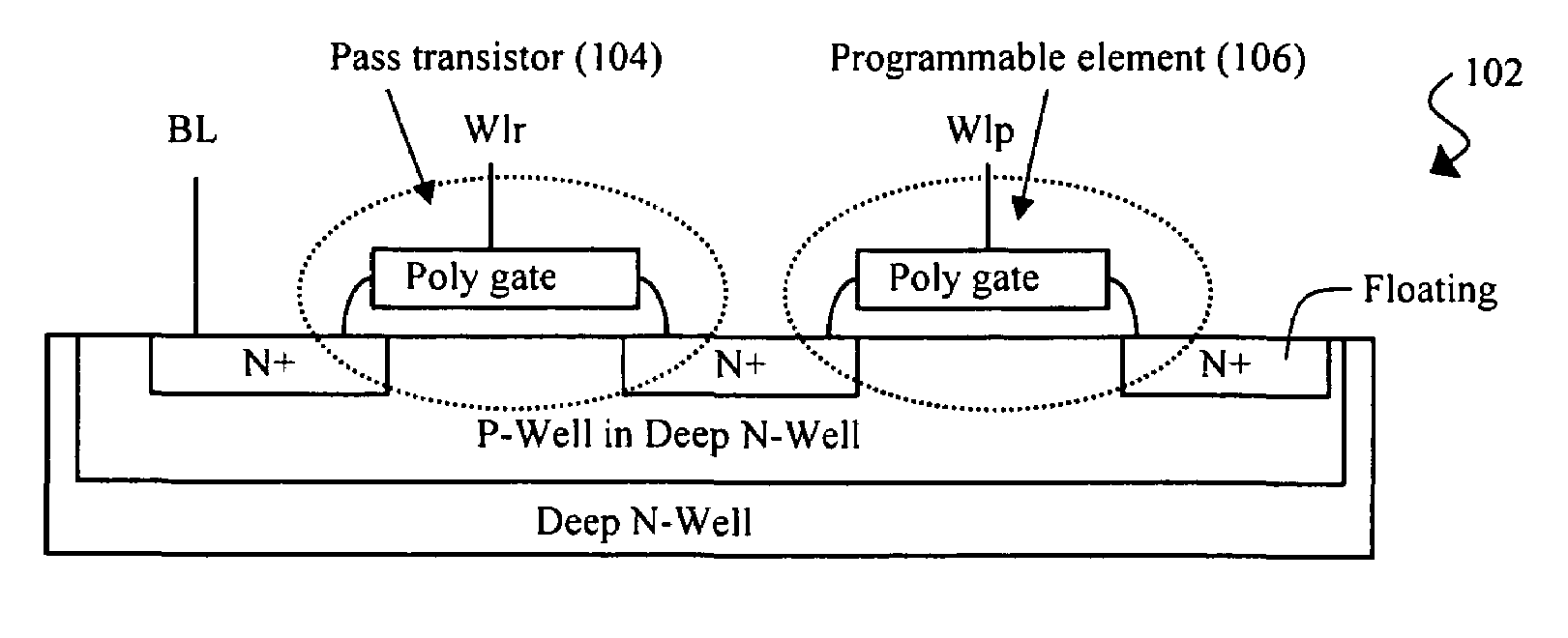
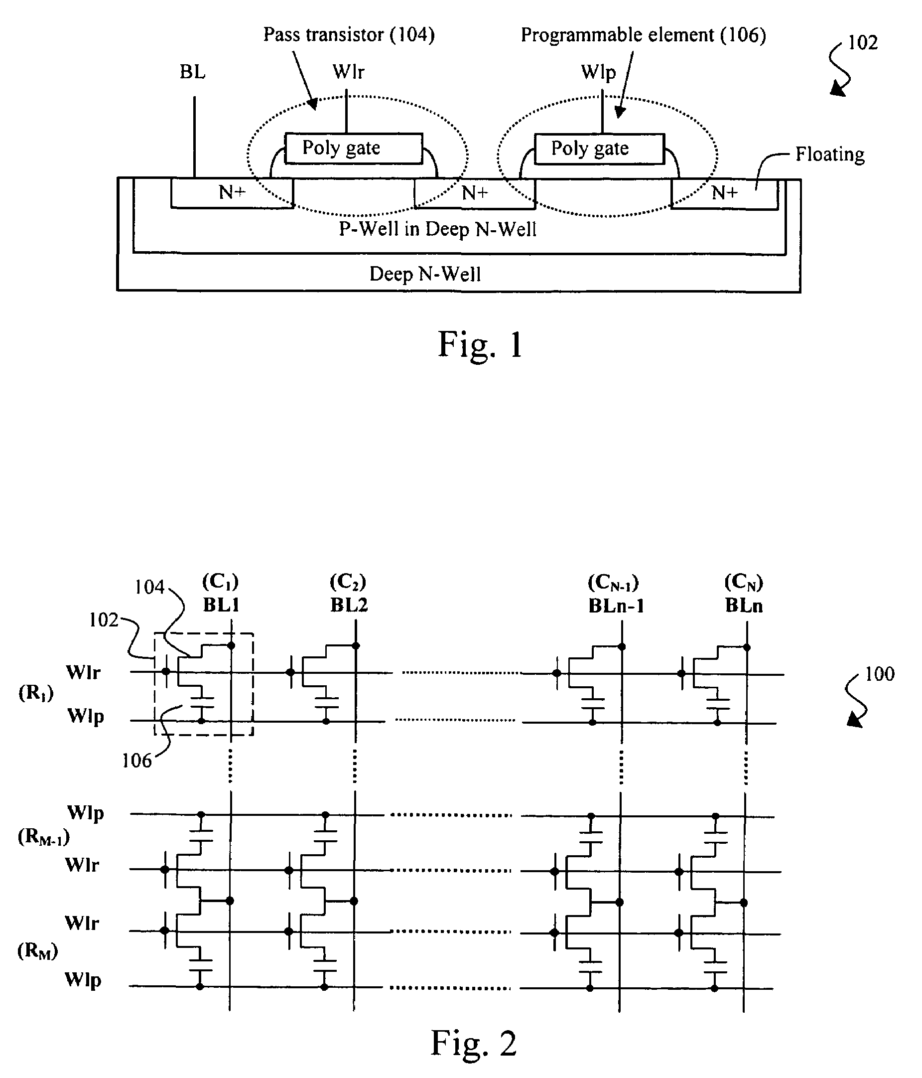
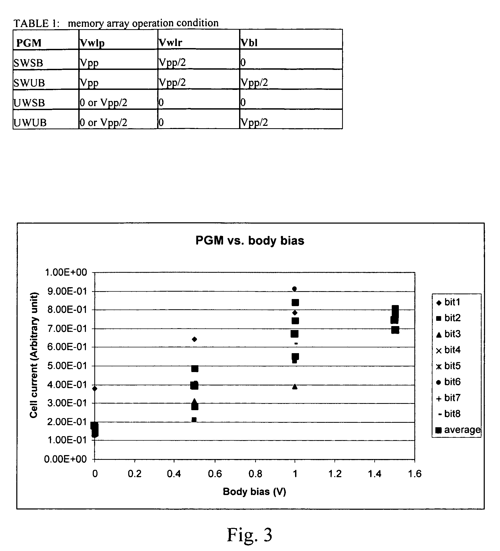
Image

Examples
Embodiment Construction
[0015]In the following description, several specific details are presented to provide a thorough understanding of the embodiments of the invention. One skilled in the relevant art will recognize, however, that the invention can be practiced without one or more of the specific details, or in combination with or with other components, etc. In other instances, well-known implementations or operations are not shown or described in detail to avoid obscuring aspects of various embodiments of the invention.
[0016]The terminology used in the description presented below is intended to be interpreted in its broadest reasonable manner, even though it is being used in conjunction with a detailed description of certain specific embodiments of the invention. Certain terms may even be emphasized below; however, any terminology intended to be interpreted in any restricted manner will be overtly and specifically defined as such in this Detailed Description section.
[0017]Reference throughout the speci...
PUM
 Abstract
Description
Claims
Application Information