Semiconductor memory device which controls refresh of a memory array in normal operation

a memory array and memory technology, applied in the direction of information storage, static storage, digital storage, etc., can solve the problems of insufficient data retention, insufficient refresh period 2sup>m/sup>t, and insufficient refresh period for actual value, so as to reduce consumption current, improve data retention characteristics, and simple configuration

Active Publication Date: 2008-12-30
MICRON TECH INC
View PDF6 Cites 4 Cited by
  • Summary
  • Abstract
  • Description
  • Claims
  • Application Information

AI Technical Summary

Benefits of technology

[0010]According to the semiconductor device of the present invention, when the refresh request is received, n bits among the n+1 bit count value are used to designate a row address, and 1 bit is used as the dummy bit. Then, the value of the dummy bit changes in response to operation of the N-ary counter to correspondingly control whether or not refresh is performed, so that a period during which refresh is performed and a period during which refresh is not performed appear alternately. Thus, refresh timing of each word line is controlled in accordance with the position of the dummy bit and setting of N for the N-ary counter so as to finely control the refresh period. Accordingly, the refresh period is adjusted so as to be adapted to the actual value of the data retention time of the memory cell, and it is possible to optimize both the data retention characteristics and the consumption current.
[0018]As descried above, according to the present invention, the refresh counter to which the dummy bit is assigned in addition to n bits included in the row address is used and the N-ary counter is configured, so as to control whether or not refresh is performed according to a value of the dummy bit. Therefore, the number of word lines being refreshed is finely controlled at every refresh timing, and the refresh period can be freely adjusted. Accordingly, a semiconductor memory device capable of achieving both the excellent data retention characteristics and the reduction of the consumption current can be realized with a simple configuration.

Problems solved by technology

However, storage capacity of the DRAM is increased recently, so the refresh period 2m·t is likely to be insufficient for data retention characteristics of the memory cell.
However, when reducing the refresh period to half, it is assumed that the refresh period is likely to be too short for the actual value of the data retention time of the memory cell while slightly reduction thereof is sufficient in reality.
That is, in the configuration in which one word line is refreshed at every refresh interval, it is insufficient in terms of the data retention characteristics of the memory cell, however in the configuration in which two word lines are refreshed, the frequency of the refresh is likely to be large so that extra current is consumed.
If the memory cell has an actual data retention time which corresponds to refresh for about 1.5 word lines at every refresh interval, it is difficult to correspondingly adjust the refresh period, and therefore it is a problem that large current is consumed in refresh operation of the DRAM.

Method used


Image

  • Semiconductor memory device which controls refresh of a memory array in normal operation
  • Semiconductor memory device which controls refresh of a memory array in normal operation
  • Semiconductor memory device which controls refresh of a memory array in normal operation

Examples


first embodiment

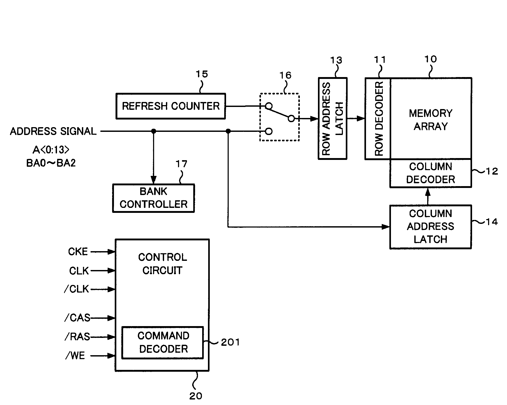
[0034]First, a configuration and operation of a DRAM of a first embodiment will be described. FIG. 1 is a block diagram showing a principal configuration of the DRAM of the first embodiment. The DRAM shown in FIG. 1 includes a memory array 10 having a large number of memory cells for storing data. Each memory cell included in the memory array 10 is formed at each intersection of a plurality of word lines and a plurality of bit lines arranged in a matrix form. The entire memory array 10 is divided into a plurality of banks (not shown) having the same size and the same configuration, and read / write operation can be controlled for each bank individually.

[0035]In the principal configuration shown in FIG. 1, a row decoder 11, a column decoder 12, a row address latch 13, a column address latch 14, a refresh counter 15, a switch unit 16 and a bank controller 17 are provided in addition to the memory array 10, and a control circuit 20 for controlling operation of these elements is provided....

second embodiment

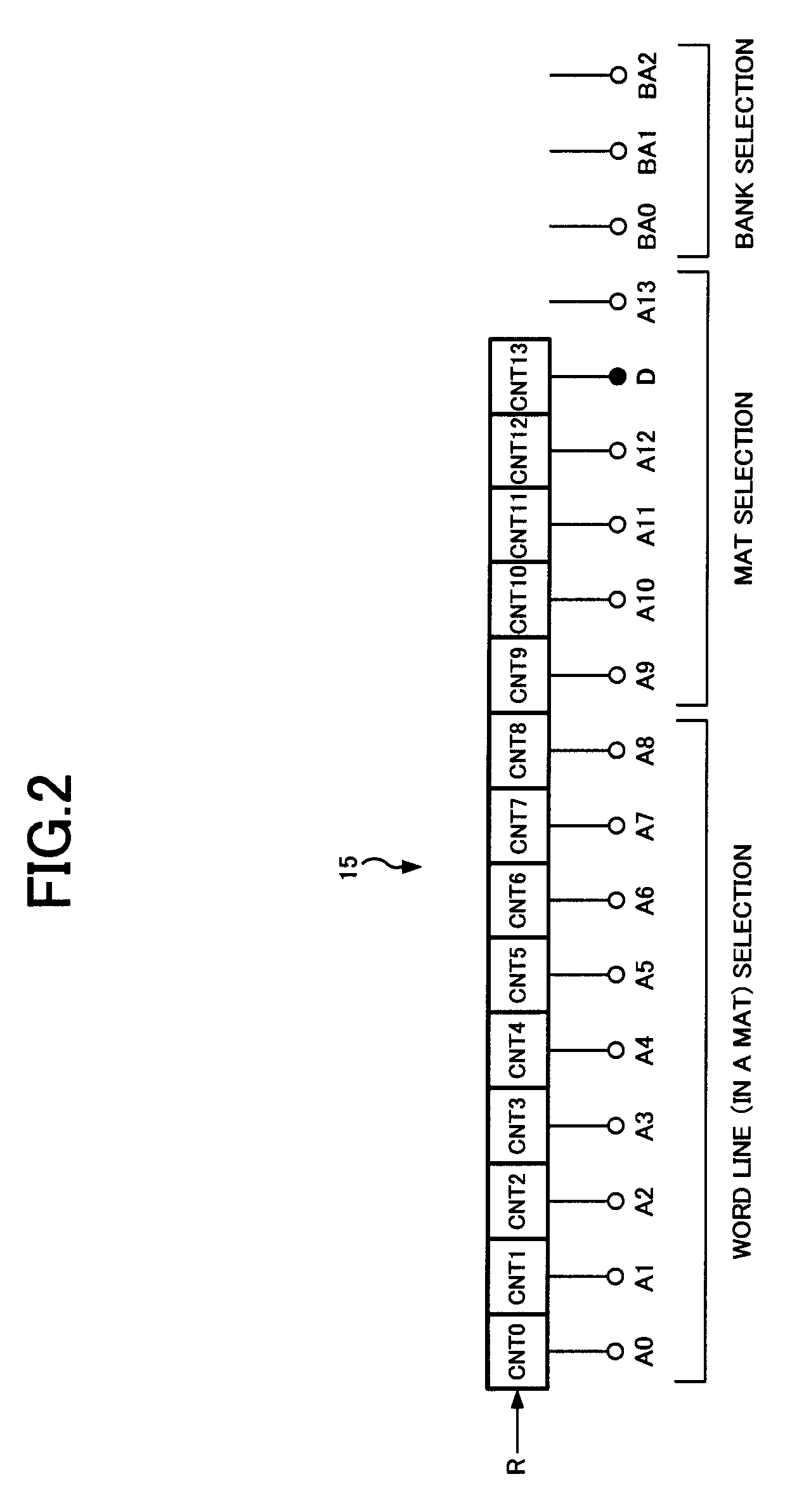
[0054]Next, a configuration and operation of a DRAM of a second embodiment will be described. A principal configuration of the second embodiment is the same as that of the first embodiment, so description thereof will be omitted. Meanwhile, a relation between the refresh counter 15 and the row address in the second embodiment is different from that in the first embodiment, so description thereof will be made with reference to FIG. 5. As shown in FIG. 5, the refresh counter 15 of the second embodiment has the same configuration as the first embodiment in the respect that 1-bit counters CNT0 to CNT13 are connected in 14 stages and a 14-bit count value is output. On the other hand, in the second embodiment, the third stage counter CNT2 of the refresh counter 15 is assigned to the dummy bit D, and the other counters CNT0, CNT1, CNT3 to CNT13 are assigned to lower 13 bits A0 to A12 of the row address. That is, it differs in that the dummy bit D is located at the most significant bit in F...

third embodiment

[0062]Next, a configuration and operation of a DRAM of a third embodiment will be described. A principal configuration and a relation between the refresh counter 15 and the row address are the same as those of the second embodiment. In the third embodiment, the assigned row address is used similarly as the second embodiment, but it is a feature that control is performed such that the most significant bit A13 of the row address is switched between redundant and non-redundant states in refresh operation.

[0063]An example of refresh operation of the third embodiment will be described with reference to FIGS. 9 to 11 corresponding to FIGS. 6 to 8 of the second embodiment. In FIGS. 9 to 11, the refresh counter 15 operates in the same condition as FIGS. 6 to 9, and cases in which the N-ary counter 15a is set to quinary (FIG. 9), senary (FIG. 10) and septenary (FIG. 11) respectively are compared.

[0064]First, in a case of N=5 shown in FIG. 9, the bit A13 becomes non-redundant when counters CN...


PUM


Abstract

A semiconductor memory device is comprised of a refresh counter for sequentially generating a count value indicating one or more row addresses corresponding to one or more word lines to be refreshed when receiving a refresh request at a predetermined interval in normal operation, in which the refresh counter includes n+1 stage counters assigned to n bits included in the row address and a dummy bit not included in the row address, and a counter portion from the least significant bit to the dummy bit forms an N-ary counter, so as to control whether or not refresh is performed in response to a value of the dummy bit when receiving the refresh request.

Description

BACKGROUND OF THE INVENTION[0001]1. Field of the Invention[0002]The present invention relates to a semiconductor memory device which controls refresh of a memory array in normal operation, and particularly relates to a semiconductor memory device such as a DRAM (Dynamic Random Access Memory) in which when receiving a refresh request at a predetermined refresh interval, one or more word lines selected based on a count value of a refresh counter can be refreshed.[0003]2. Description of the Related Art[0004]Generally, each memory cell of a DRAM should be refreshed at a predetermined refresh period in order to retain data stored as electric charge in the memory cell. In normal operation of an arbitrary bank of the DRAM, a refresh counter counts up a row address at every refresh interval defined in the specification and refresh is sequentially performed for the row address indicated by the count value. For example, on the assumption that 2m word lines corresponding to an m-bit row addres...

Claims


Application Information

Patent Timeline
Patent Type & Authority Patents(United States)
IPC IPC(8): G11C7/00
CPCG11C11/406G11C11/40611G11C11/40622G11C2211/4061
Inventor KOSHIKAWA, YASUJI
Owner MICRON TECH INC
Why Eureka
Try Eureka