Semiconductor devices having phase change memory cells, electronic systems employing the same and methods of fabricating the same
What is AI technical title?
AI technical title is built by PatSnap AI team. It summarizes the technical point description of the patent document.
a technology of phase change memory and semiconductor devices, applied in the direction of semiconductor devices, bulk negative resistance effect devices, electrical appliances, etc., can solve the problems of affecting the operation of memory programming, and affecting the accuracy of memory programming, so as to achieve stable operation and prolong the operation life
Active Publication Date: 2009-01-27
SAMSUNG ELECTRONICS CO LTD
View PDF31 Cites 37 Cited by
Summary
Abstract
Description
Claims
Application Information
AI Technical Summary
This helps you quickly interpret patents by identifying the three key elements:
Problems solved by technology
Method used
Benefits of technology
Benefits of technology
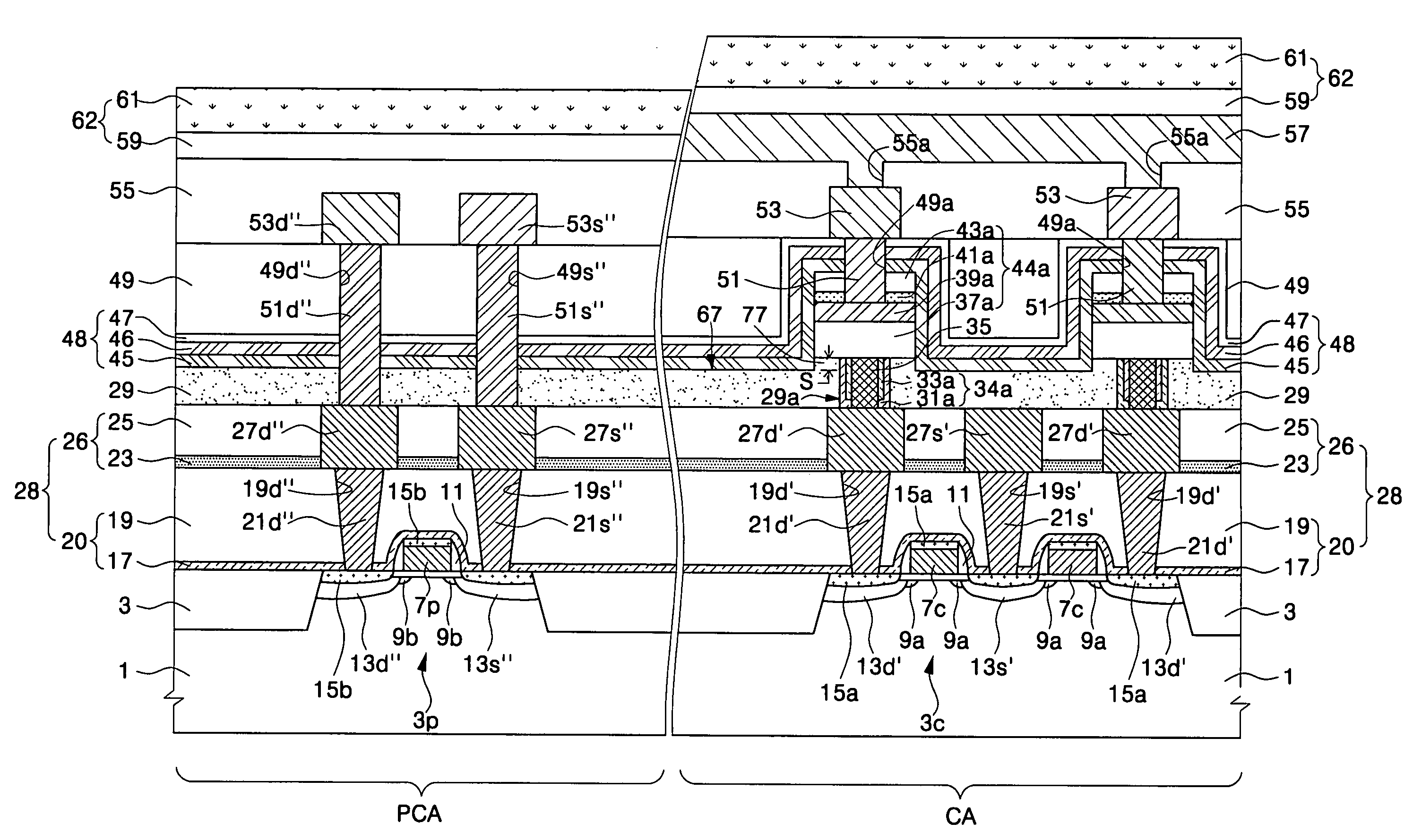
[0007]A phase-change memory device has an oxidation barrier layer to protect against memory cell contamination or oxidation and a method of manufacturing the same. In one embodiment, a semiconductor memory device comprises a molding layer overlying a semiconductor substrate. The molding layer has a protrusion portion vertically extending from a top surface thereof. The device further includes a phase-changeable material pattern adjacent the protrusion portion and a lower electrode electrically connected to the phase-changeable material pattern. According to one aspect of the present invention, an oxidation barrier layer may cover an area where a sidewall of the phase-changeable material pattern and a sidewall of the protrusion portion adjoin. More stable operation and a longer operational lifetime of the phase-change memory device are some of the benefits of the present invention.
Problems solved by technology
During a fabrication of the memory device, and during its operational life in use, these interfaces may become contaminated or oxidized.
Since the operation of phase-changeable memory depends on distinguishing between the memory cell being “on” or “off” based on the cell's resistance to current flow, contamination or oxidation jeopardizes the accuracy of memory programming.
Method used
Image
Click on the blue label to locate the original text in one second.
Reading with bidirectional positioning of images and text.
Examples
examples
[0073]FIG. 17 is a graph illustrating set / reset resistance characteristics of the phase-change memory cells fabricated according to the present invention and the conventional art. In FIG. 17, a horizontal axis represents a diameter D of the phase-change material patterns, and a vertical axis represents a resistance R of the phase-change resistors. In the graph of FIG. 17, the data indicated by reference letters “NR” and “NS” represent a reset resistance and a set resistance of the conventional phase-change resistors fabricated without an oxidation barrier layer, respectively. The data indicated by reference letters “SR” and “SS” represent a reset resistance and a set resistance of the phase-change resistors covered with a single oxidation barrier layer, respectively. Further, the data indicated by reference letters “DR” and “DS” represent a reset resistance and a set resistance of the phase-change resistors covered with a double oxidation barrier layer, respectively. The phase-chang...
PUM
Abstract
In one embodiment, a phase-change memory device has an oxidation barrier layer to protect against memory cell contamination or oxidation and a method of manufacturing the same. In one embodiment, a semiconductor memory device comprises a molding layer overlying a semiconductor substrate. The molding layer has a protrusion portion vertically extending from a top surface thereof. The device further includes a phase-changeable material pattern adjacent the protrusion portion and a lower electrode electrically connected to the phase-changeable material pattern.
Description
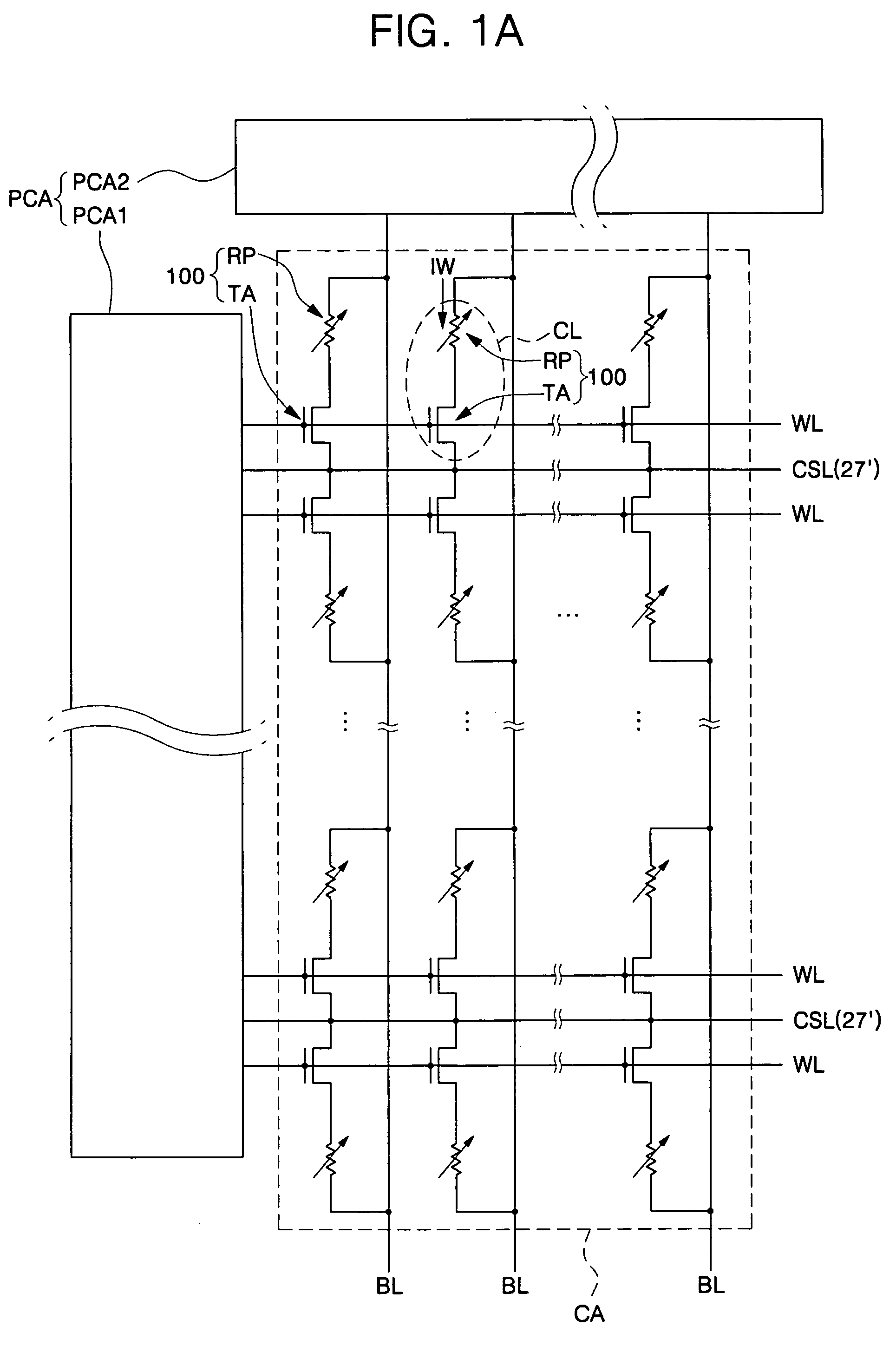
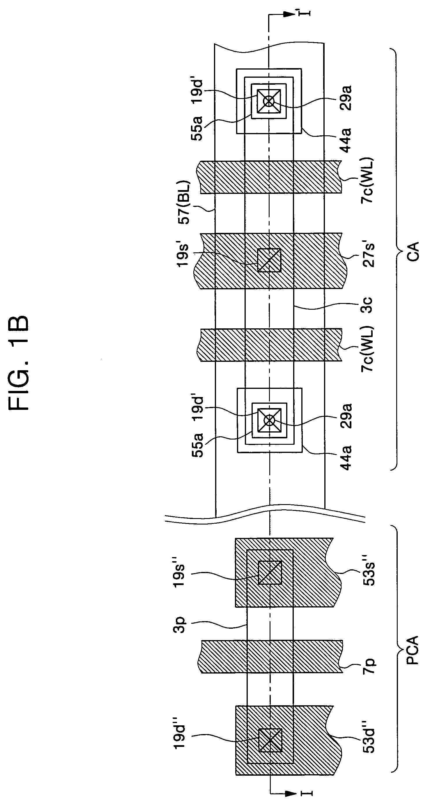
CROSS-REFERENCE TO RELATED APPLICATION[0001]The present application is a continuation-in-part of U.S. patent application Ser. No. 11 / 027,255, filed Dec. 30, 2004, now issued as U.S. Pat. No. 7,411,208, which claims priority from Korean Patent Application No. 2004-37965, filed on May 27, 2004. Also, the present application claims the priority from Korean Patent Application Nos. 2004-105905 and 2005-31662, filed Dec. 14, 2004 and Apr. 15, 2005, respectively. The disclosures of all of the above applications are incorporated herein by reference in their entirety.BACKGROUND OF THE INVENTION[0002]1. Field of the Invention[0003]The invention relates to a semiconductor memory device and methods of fabricating the same, and more particularly, to a phase-change memory device and methods of fabricating the same.[0004]2. Description of Related Art[0005]The use of phase-changeable materials for electronic memory applications is known in the art and is disclosed, for example, in U.S. Pat. Nos. 6,...
Claims
Application Information
Patent Timeline
Application Date:The date an application was filed.
Publication Date:The date a patent or application was officially published.
First Publication Date:The earliest publication date of a patent with the same application number.
Issue Date:Publication date of the patent grant document.
PCT Entry Date:The Entry date of PCT National Phase.
Estimated Expiry Date:The statutory expiry date of a patent right according to the Patent Law, and it is the longest term of protection that the patent right can achieve without the termination of the patent right due to other reasons(Term extension factor has been taken into account ).
Invalid Date:Actual expiry date is based on effective date or publication date of legal transaction data of invalid patent.

