Method to optimize the manufacturing of interconnects in microelectronic packages

a technology of microelectronic packaging and manufacturing methods, applied in the direction of cad circuit design, program control, instruments, etc., can solve the problems of defect-free and reliable interconnection between an ic and a substrate, and the presence of defects

Inactive Publication Date: 2009-01-27
IBM CORP
View PDF9 Cites 3 Cited by
  • Summary
  • Abstract
  • Description
  • Claims
  • Application Information

AI Technical Summary

Problems solved by technology

A first type of defect that may be present immediately after manufacturing is an open circuit, for example due to the fact that a solder bump is too small to contact both the pad on the IC side and the pad on the substrate side.
Forming defect-free and reliable interconnects between an IC and a substrate is difficult, in part because of the high variability in many critical parameters, such as the planarity of the substrate, the volume of solder bumps, IC alignment, etc.

Method used


Image

  • Method to optimize the manufacturing of interconnects in microelectronic packages
  • Method to optimize the manufacturing of interconnects in microelectronic packages
  • Method to optimize the manufacturing of interconnects in microelectronic packages

Examples


Embodiment Construction

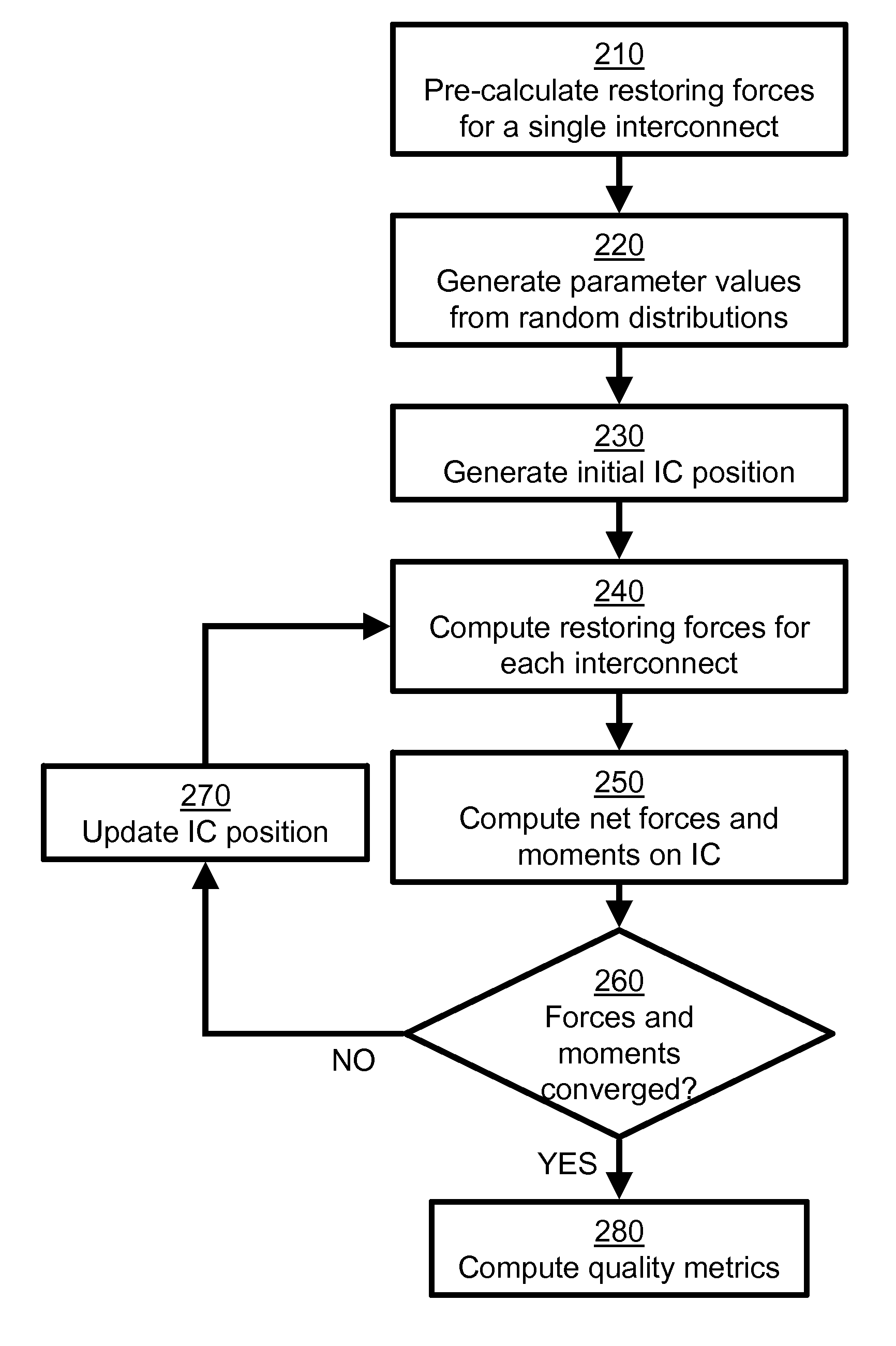
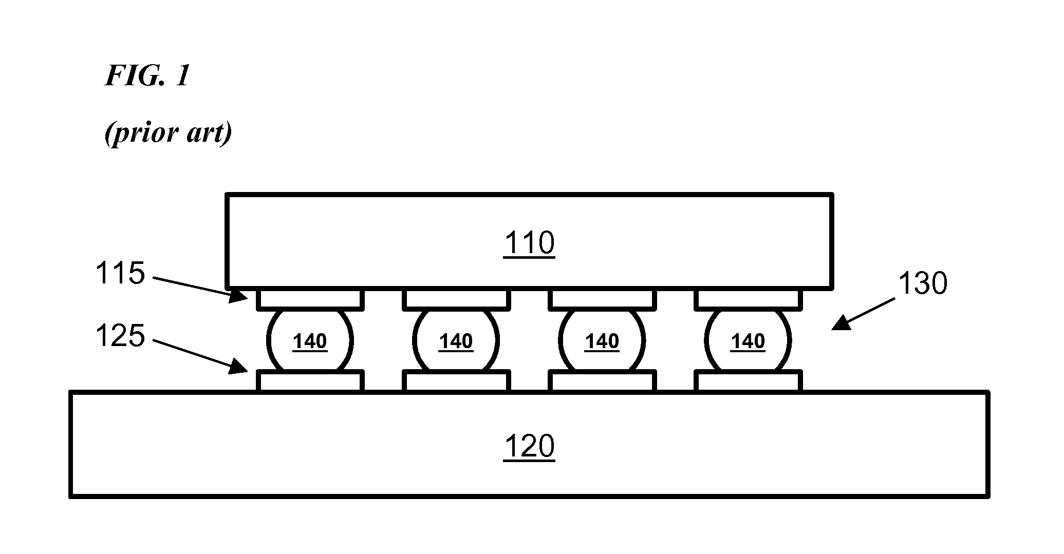
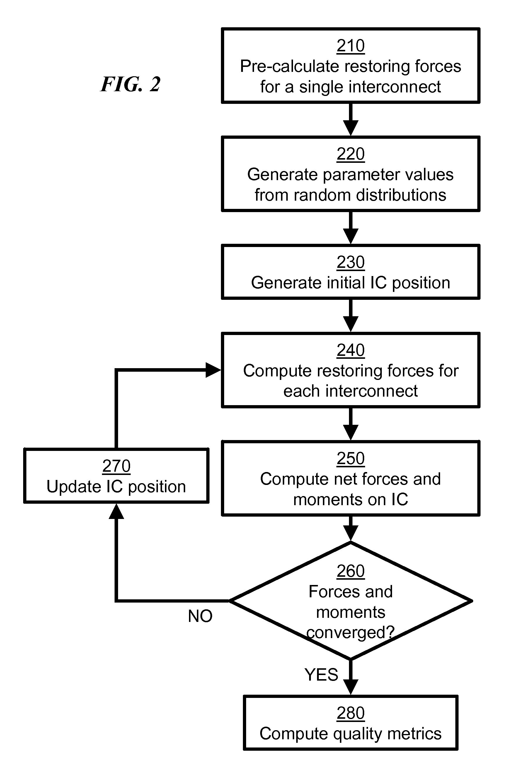
[0010]FIG. 1 shows a side view of a prior art integrated circuit and printed circuit board to which embodiments of the invention may be applied. The integrated circuit 110 is positioned over a substrate 120. The integrated circuit 110 includes pads 115 and substrate includes pads 125. Pads 115 and 125 are connected by interconnects 130 formed by melting and then solidifying solder bumps 140, thus forming solder joints. While the drawing only shows four interconnects aligned in a row, industry-standard ICs include hundreds of interconnects, typically arranged in a matrix over the entire surface of the IC.

[0011]The physical parameters of the process of forming solder joints depend partly on the type of solder used. Typically, a temperature sufficient for the solder to undergo a transition to the liquid phase is required for reliable formation of interconnects. For example, traditional eutectic tin-lead solder (Pb 37%, Sn 63%) has a melting point of 183° C. The transition toward lead-f...


PUM


Abstract

A method for optimizing the manufacturing of interconnects in microelectronic packages in the presence of sources of process variability. The method can estimate the contribution of multiple parameter to the quality of the interconnects, enabling the optimization of the manufacturing process.

Description

FIELD OF THE INVENTION[0001]This invention relates to integrated circuit packaging, and in particular to the formation of interconnects between a semiconductor product, such as a packaged integrated circuit (IC), and a substrate, such as a printed circuit board (PCB).BACKGROUND[0002]Modem microelectronic packages such as flip-chip ball grid array (FCBGA) packages may include several hundred closely spaced interconnects, formed as solder joints distributed over the entire area of the integrated circuit (IC). Each interconnect includes a solder bump which connects a pad located on the IC with a corresponding pad on a substrate. Known substrates include for example printed circuit boards (PCBs) formed from organic laminates, and ceramic substrates.[0003]Interconnects must be formed by a process that is both defect-free and reliable over the long term. A first type of defect that may be present immediately after manufacturing is an open circuit, for example due to the fact that a solder...

Claims


Application Information

Patent Timeline
Patent Type & Authority Patents(United States)
IPC IPC(8): G06F17/50
CPCG06F17/5068G06F2217/40G06F30/39G06F2113/18
Inventor DUCHESNE, ERICSYLVESTRE, JULIEN
Owner IBM CORP
Why Eureka
Try Eureka