Nonvolatile semiconductor storage device and manufacturing method therefor

a semiconductor storage device and non-volatile technology, applied in the direction of drying machines, lighting and heating apparatus, furnaces, etc., can solve the problems of data write failure and interference between memory cells, and achieve the effect of reducing interference between memory cells and easy control of capacitive coupling ratio

Inactive Publication Date: 2009-02-10
KK TOSHIBA
View PDF10 Cites 6 Cited by
  • Summary
  • Abstract
  • Description
  • Claims
  • Application Information

AI Technical Summary

Benefits of technology

[0007]An advantage of an aspect of the present invention is to provide a nonvolatile semiconductor storage device which reduces interference between memory cells caused by miniaturization and can easily control the capacitive coupling ratio between the memory cells in order to solve the above-described problem.

Problems solved by technology

This produces the proximity effect in memory cells and causes interference between memory cells.
Accordingly, a threshold difference (ΔVTH) narrows between a state wherein data is written and a state wherein data is erased, thus resulting in a data write failure.

Method used


Image

  • Nonvolatile semiconductor storage device and manufacturing method therefor
  • Nonvolatile semiconductor storage device and manufacturing method therefor
  • Nonvolatile semiconductor storage device and manufacturing method therefor

Examples


first embodiment

(Second Modification of First Embodiment)

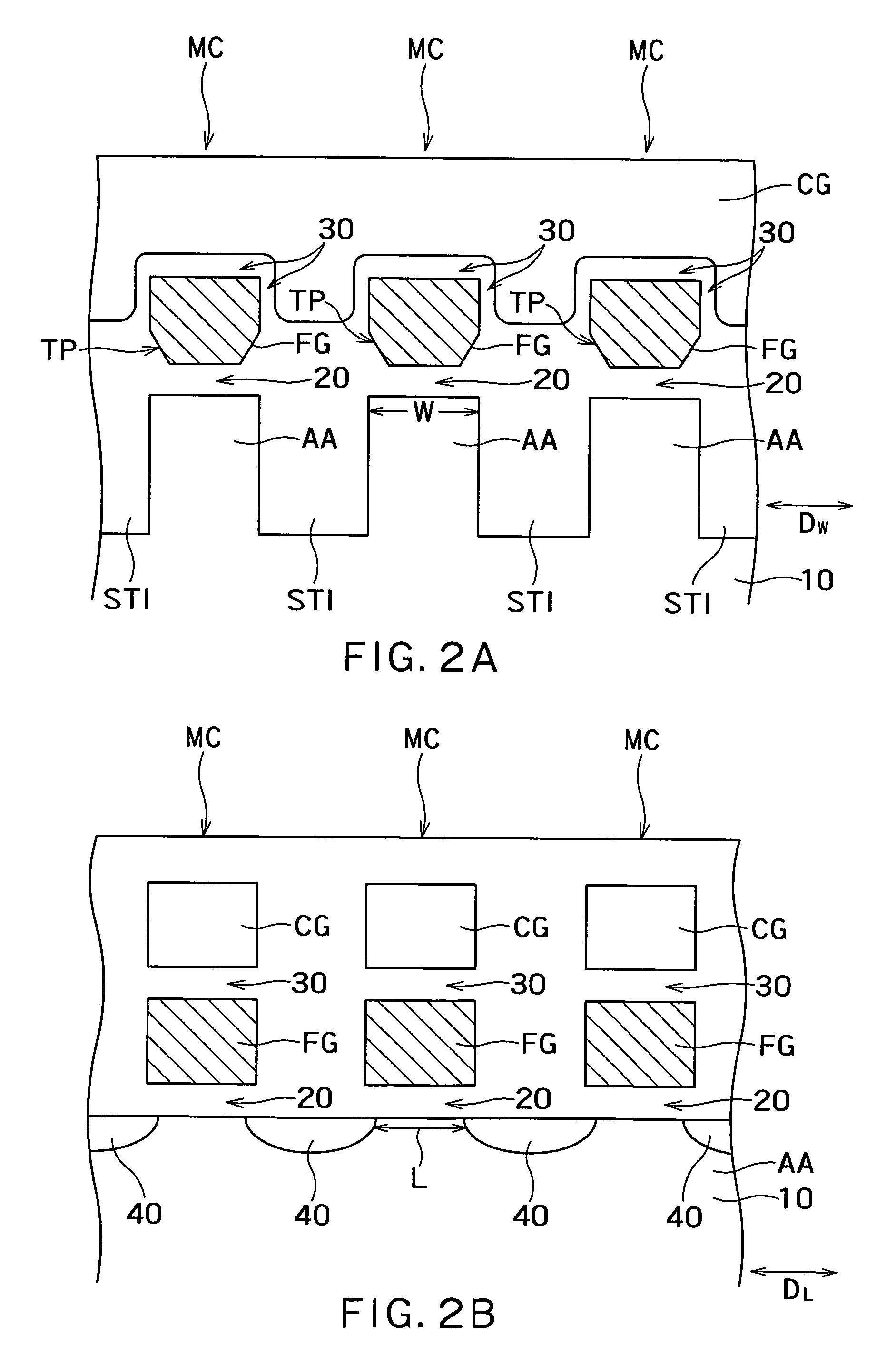
[0071]FIG. 11 is a sectional view showing the second modification of the first embodiment according to the present invention. In this modification, only one of two side walls of each floating gate electrode FG is etched by oblique etching. As described above, even if each taper TP is formed only at one of two side walls of the corresponding floating gate electrode FG, the width of the lower hem of the floating gate electrode FG becomes narrower than the width of the corresponding active area AA. Accordingly, the same effects as in the first embodiment can be obtained. According to this modification, it is only necessary to etch one of two side walls of each floating gate electrode FG by RIE. Thus, the manufacturing cost can be suppressed.

Second Embodiment

[0072]FIGS. 12 to 14 are sectional views showing the flow of a method of manufacturing a NAND-type flash memory 100 according to the second embodiment of the present invention. FIGS. 12 to 14...

second embodiment

(Modification of Second Embodiment)

[0077]The second embodiment has been explained as a method of forming each taper TP at two side walls of the corresponding floating gate electrode FG in a section taken in the channel width direction DW. However, if etching in a direction DL is performed by RIE using the same reactive gas, similar tapers are automatically formed in a section taken in the direction DL as well. If the etching in the direction DL is performed by RIE using a reactive gas with a low reactivity to Ge, no tapers are formed in a section taken in the direction DL. As described above, in the second embodiment as well, a direction in which tapers are formed can be selected. The second embodiment is also advantageous in terms of manufacture in that there is no difference in the number of steps required for RIE between a case wherein tapers are formed in both sections taken in the directions DL and DW and a case wherein tapers are formed in either one of sections taken in the d...

third embodiment

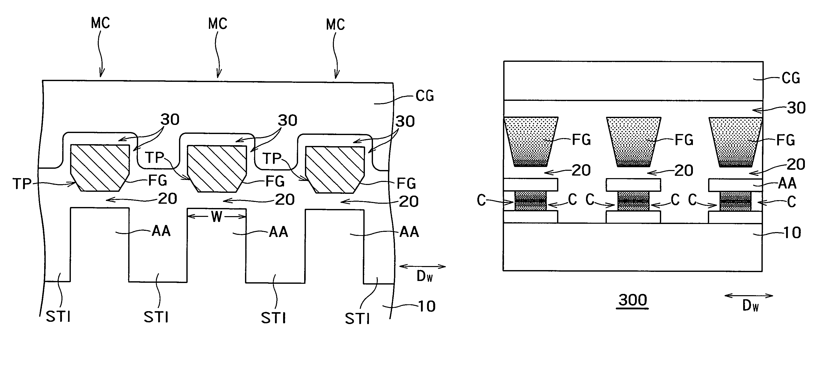
[0083]FIGS. 19(A) and 19(B) are sectional views of a NAND-type flash memory 200 (to be also simply referred to as the memory 200 hereinafter) according to the third embodiment of the present invention. FIG. 19(A) is a sectional view taken along the line A-A shown in FIG. 1; and FIG. 19(B) is a sectional view taken along the line B-B shown in FIG. 1. In the third embodiment, recesses C are formed in side walls of active areas AA in a section taken in a channel width direction DW, as shown in FIG. 19(A). With these recesses C, the width of at least a part of the sides (body) of each active area AA is narrower than that of the top surface of the active area AA, in a section taken in a direction perpendicular to a direction in which STIs extend. Each recess C is formed at a depth equal to that where an off-leak current flows in the active area AA. More specifically, the depth is ideally equal to or deeper than that where an extension of a diffusion layer is located. Accordingly, an off-...


PUM


Abstract

A nonvolatile semiconductor storage device includes a semiconductor substrate; a plurality of isolation regions formed in the semiconductor substrate; an element-forming region formed between adjacent isolation regions; a first gate insulating film provided on the element-forming region; a floating gate electrode which is provided on the first gate insulating film and in which a width of a lower hem facing the element-forming region is narrower than a width of the element-forming region in a section taken in a direction perpendicular to a direction in which the isolation regions extend; a second gate insulating film provided on the floating gate electrode; and a control gate electrode provided on the second gate insulating film.

Description

CROSS-REFERENCE TO RELATED APPLICATION[0001]This application is based upon and claims the benefit of priority from the prior Japanese Patent Applications No. 2005-86803, filed on Mar. 24, 2005, the entire contents of which are incorporated herein by reference.BACKGROUND OF THE INVENTION[0002]1. Field of the Invention[0003]The present invention relates to a nonvolatile semiconductor storage device and manufacturing method therefor.[0004]2. Background Art[0005]Since a NAND-type flash memory leaves bit line control to a selection transistor, it can be made smaller in cell area than a NOR-type flash or DRAM. Thus, NAND-type flash memories can be manufactured at a low cost.[0006]However, as NAND-type flash memories are being miniaturized, the spacing between memory cells (the width of an STI) decreases with a decrease in size of memory cells. This produces the proximity effect in memory cells and causes interference between memory cells. Interference between memory cells acts to average ...

Claims


Application Information

Patent Timeline
Patent Type & Authority Patents(United States)
IPC IPC(8): H01L29/788
CPCH01L27/115H01L27/11521H01L29/42324H01L29/7881H10B69/00H10B41/30F26B3/04F26B21/08F26B21/10F26B2200/16
Inventor WATANABE, HIROSHIKINOSHITA, ATSUHIROTAKASHIMA, AKIRAHAGISHIMA, DAISUKE
Owner KK TOSHIBA
Why Eureka
Try Eureka