Semiconductor device and manufacturing method of the same

a technology of semiconductor devices and manufacturing methods, applied in the direction of semiconductor devices, basic electric elements, electrical appliances, etc., can solve the problems of increasing the gate resistance, reducing the yield rate, and not being able to obtain particular characteristics of the d-fet constituting the switch, etc., to achieve controllability and stability of the threshold voltage, reduce the increase in the gate resistance of the d-fet, and improve the yield rate

Inactive Publication Date: 2009-02-24
PANASONIC CORP
View PDF4 Cites 2 Cited by
  • Summary
  • Abstract
  • Description
  • Claims
  • Application Information

AI Technical Summary

Benefits of technology

[0047]According to this structure, in the semiconductor device according to the present invention, the first gate electrode which is a gate electrode of the E-FET and the second gate electrode which is a gate electrode of the D-FET are made of different materials. Thereby, by using a material having less reactivity to the first Schottky layer caused by an effect such as a process temperature, as the material constituting the gate electrode of the E-FET, it is possible to improve the controllability and the stability of a threshold voltage required for the E-FET. Further, by using a material having low resistance as the material constituting the gate electrode of the D-FET, it is possible to reduce the gate resistance of the D-FET and to improve the characteristics. Thereby, the semiconductor device according to the present invention can realize the characteristics required for both of the E-FET and the D-FET.
[0062]According to this structure, the source electrodes and the drain electrodes of the E-FET and the D-FET are simultaneously formed of the identical material as the gate electrode of the D-FET. Thereby, the process steps can be reduced. This enables to reduce the process cost.

Problems solved by technology

With such a structure, the gate resistance increases, whereby the characteristics of the D-FET constituting a switch can not be sufficiently obtained particularly.
If the threshold voltage fluctuates, the required characteristics can not be achieved, causing the yield to drop.
That is, a conventional semiconductor device, in which E / D-FET are mounted in a mixed manner, can not be realized while achieving the characteristics required for both of the E-FET and the D-FET.

Method used


Image

  • Semiconductor device and manufacturing method of the same
  • Semiconductor device and manufacturing method of the same
  • Semiconductor device and manufacturing method of the same

Examples


Embodiment Construction

[0081]Hereinafter, a semiconductor device according to an embodiment of the present invention is described with reference to the drawings.

[0082]In a semiconductor device according to the embodiment of the present invention, a gate electrode of an E-FET and a gate electrode of a D-FET are made of different materials. This enables to improve the characteristics of the E-FET and the D-FET.

[0083]First, a structure of the semiconductor device according to the embodiment of the present invention is described.

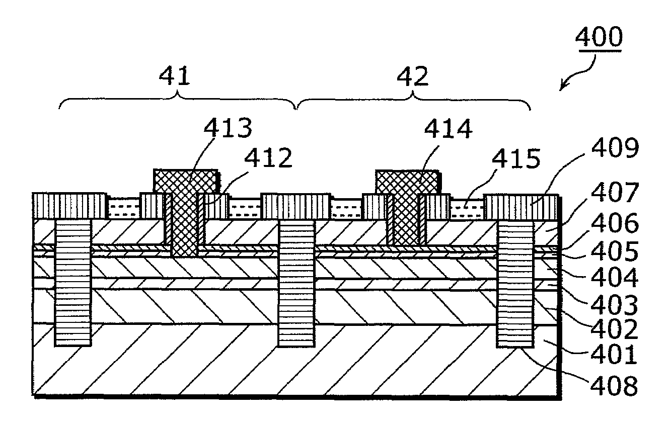
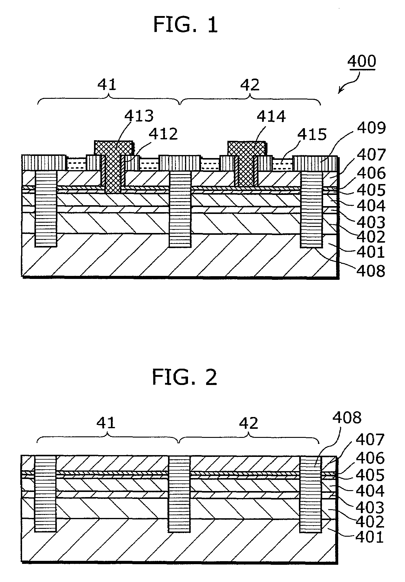
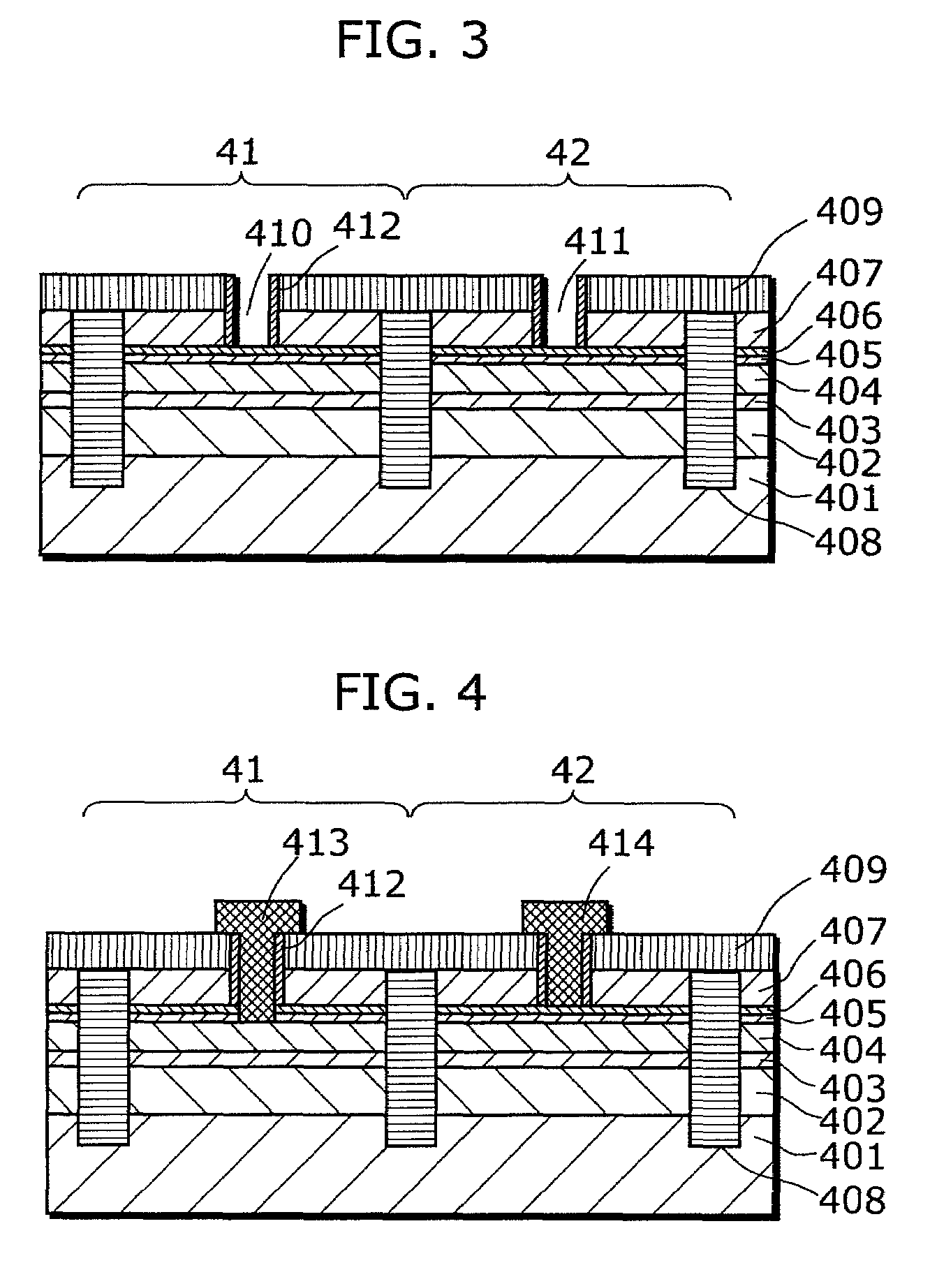
[0084]FIG. 8 is a cross sectional view showing the structure of the semiconductor device according to the embodiment of the present invention.

[0085]A semiconductor device 100 shown in FIG. 8 includes an E-FET region 11 in which an E-FET is formed, and a D-FET region 12 in which a D-FET is formed. The semiconductor device 100 includes a substrate 101 which is a semiconductor substrate made of semi-insulating GaAs, an epitaxial layer 110, an isolation region 111, insulating films 112 an...


PUM


Abstract

A semiconductor device according to the present invention includes: a semiconductor substrate; a channel layer formed on the semiconductor substrate; a donor layer formed on the channel layer; a first Schottky layer formed on the donor layer; a second Schottky layer formed on the first Schottky layer; a first gate electrode formed on the first Schottky layer to form a Schottky barrier junction with the first Schottky layer; a first source electrode and a first drain electrode formed so as to sandwich the first gate electrode and electrically connected to the channel layer; a second gate electrode formed on the second Schottky layer and made of a material different from the first gate electrode to form a Schottky barrier junction with the second Schottky layer; and a second source electrode and a second drain electrode formed so as to sandwich the second gate electrode and electrically connected to the channel layer.

Description

BACKGROUND OF THE INVENTION[0001](1) Field of the Invention[0002]The present invention relates to a semiconductor device and a manufacturing method of the same. In particular, the present invention relates to a semiconductor device in which two or more kinds of field-effect transistors having different threshold voltages are integrated on a compound semiconductor substrate, and to a manufacturing method of the same.[0003](2) Description of the Related Art[0004]Field-effect transistors made of GaAs (hereinafter referred to as GaAsFET) formed on semiconductor substrates have been used as power amplifiers or switches of communication equipment such as mobile telephone terminals due to its high performance. Particularly, monolithic microwave integrated circuits in which active elements such as a GaAsFET and passive elements such as a resistance element and a capacitance element are integrated (hereinafter referred to as GaAsMMIC) have been widely and practically used.[0005]In recent yea...

Claims


Application Information

Patent Timeline
Patent Type & Authority Patents(United States)
IPC IPC(8): H01L29/812
CPCH01L29/42316H01L29/66863H01L29/8128H01L29/778
Inventor KATO, YOSHIAKIANDA, YOSHIHARUTAMURA, AKIYOSHI
Owner PANASONIC CORP
Why Eureka
Try Eureka