Method for image sensor calibration and associated devices

a technology for image sensors and associated devices, applied in the field of image sensors, can solve the problems of reducing the sensitivity of a pixel, and often impractical halving the frame rate, and achieve the effect of reducing the frame rate or reducing the loss of sensitivity

Active Publication Date: 2009-03-10
STMICROELECTRONICS (RES & DEV) LTD
View PDF19 Cites 12 Cited by
  • Summary
  • Abstract
  • Description
  • Claims
  • Application Information

AI Technical Summary

Benefits of technology

[0016]In view of the foregoing background, an object of the present invention is to provide an offset cancellation method that does not incur a significant reduction in frame rate or loss of sensitivity in a pixel.
[0017]It would also be desirable for the method to be compatible with the cancellation of other sources of noise, for example kTC noise. It is also desirable to avoid storage of voltage at the pixel so that the fill factor and sensitivity of the sensor is not decreased.

Problems solved by technology

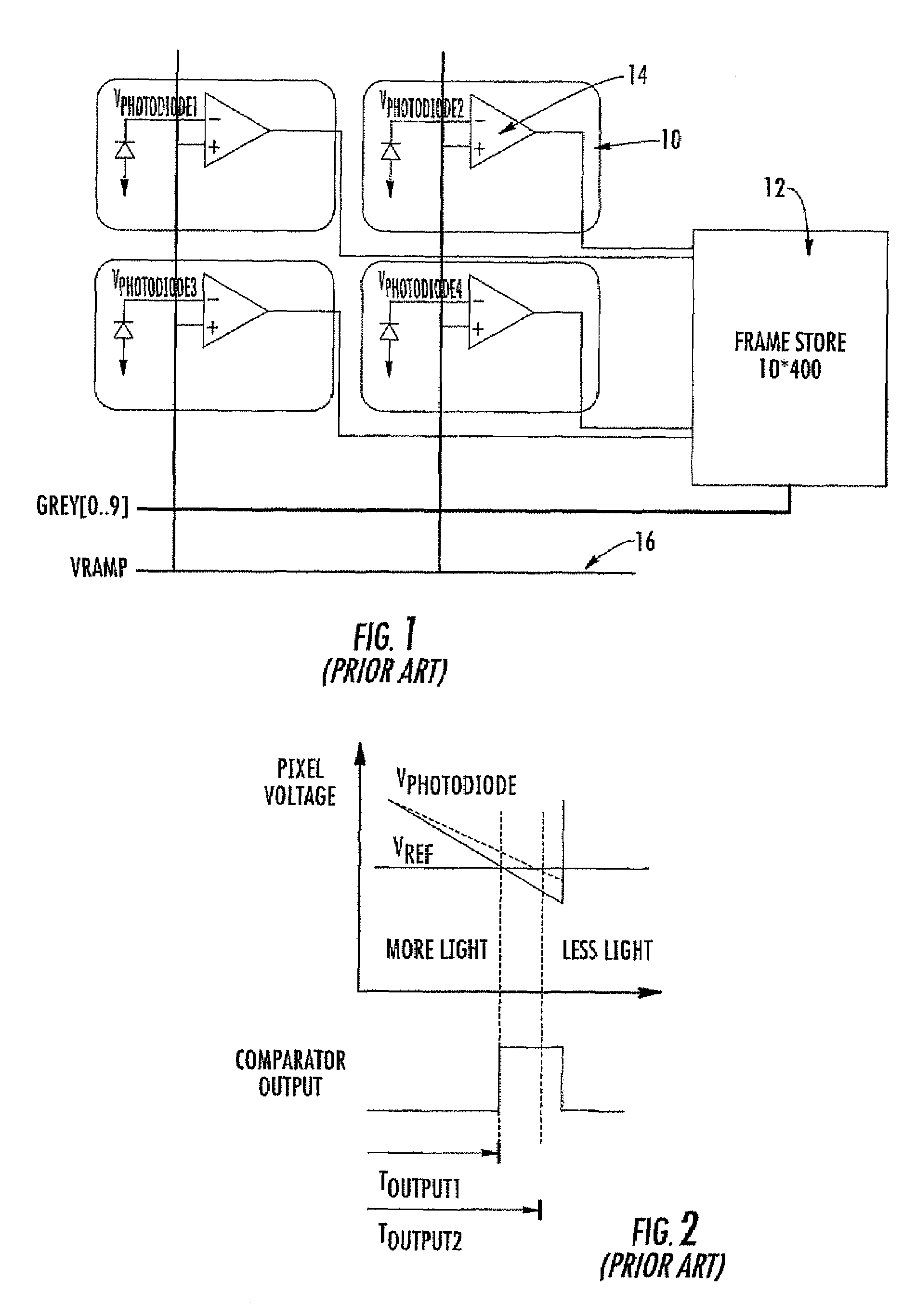
On a graph of voltage against time, an increase in incident light will result in a steeper slope.
This leads to problems since the environment (especially the sensor's temperature) will change, such as causing differences in the offsets.
However, there are some disadvantages with dark frame cancellation.
For higher speed applications, dark current is much lower and of less concern and halving the frame-rate is often impractical.
However, implementation of CDS at the pixel requires some extra space for the storage node, which reduces the amount of area in each pixel available for light collection (i.e., fill-factor), and the sensor's sensitivity is reduced.

Method used


Image

  • Method for image sensor calibration and associated devices
  • Method for image sensor calibration and associated devices
  • Method for image sensor calibration and associated devices

Examples


first embodiment

[0036]FIG. 8 illustrates a method for operating an image sensor, in which there are three phases, namely a reset phase, a calibration phase (calibrate) and an integration phase, which comprises sensor exposure and conversion of the incoming signal.

[0037]Phase 1—Reset. During this phase the RESET line (f) goes active and the pixel is reset. Hence, the voltage at the photodiode (a) remains constant. The comparator is not used, so the value of the input Vref (b) is a do not care.

[0038]The time for reset is not critical to this application. The minimum time is determined by how quickly the support circuitry can reset the pixel. The maximum time is determined by the system's frame rate. Typically, the system will use the shortest reset period possible to maximize the frame rate. A practical range for the reset period is 1 μs to 10 μs. At the end of this period the RESET line (f) goes inactive and kTC noise is put onto the pixel.

[0039]Phase 2—Calibration. For high accuracy, there should b...

second embodiment

[0045]FIG. 9 illustrates a method of operating an image sensor, which incorporates a reset phase, a calibration phase, an exposure phase and a conversion phase (convert).

[0046]The reset and calibration phases are similar to those of the first embodiment. However, the exposure and conversion phases are now treated independently rather than as a combined integration phase. This embodiment is suitable for use with an enhanced dynamic-range sensor.

[0047]Phase 3—Exposure. The Vref signal ramps during this phase. The point at which the comparator output changes is now inversely proportional to the light. This function is not linear and has the advantage that for a large amount of light 1 / Light gets smaller, but can never reach zero. The pixel's readout can never saturate. Offset time 40 gives a measure of the pixel's offset.

[0048]Phase 4—Convert. After exposure, the illumination is turned off and the reference voltage then ramps between the black value and white value. Measuring the conve...


PUM


Abstract

An image sensor includes an array of digital pixels, a first frame store for storing reference data, and a second frame store for storing image data. The reference and image data are combine to cancel an off-set of the pixels in the array. A re-set and a calibration phase are performed while a shutter is closed to obtain reference data during a calibration phase. A comparator measures an off-set time to gather information on the off-set of the pixels. During or after an exposure phase a conversion time is measured representative of the illumination on the pixel. During the calibration phase the off-set is measured. This digital technique requires a much smaller voltage swing on the pixel, and known techniques and can be performed in a shorter time. This increases the overall frame rate of the image sensor since the time taken for the reset and calibration phases is less than the time taken for the exposure phase.

Description

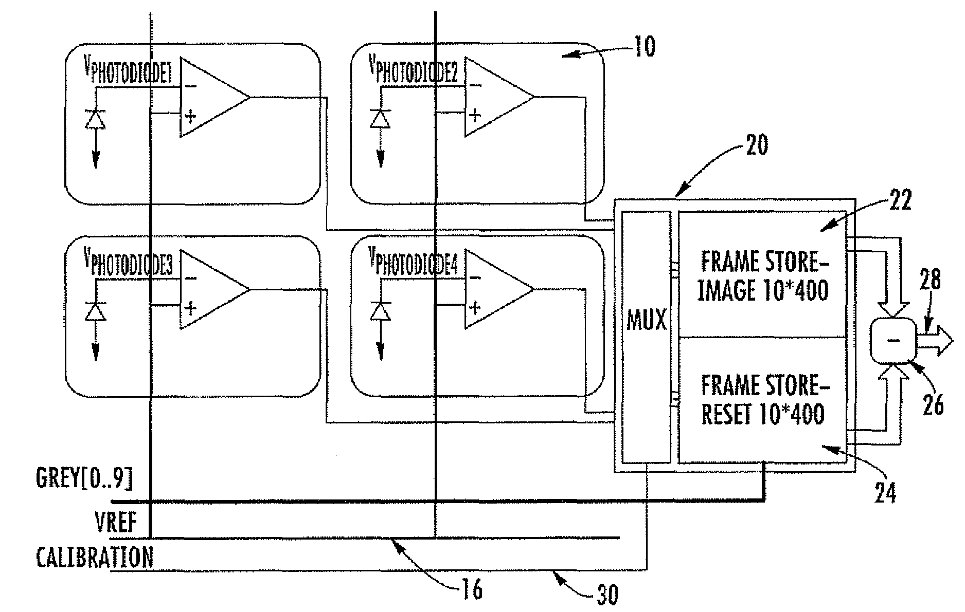
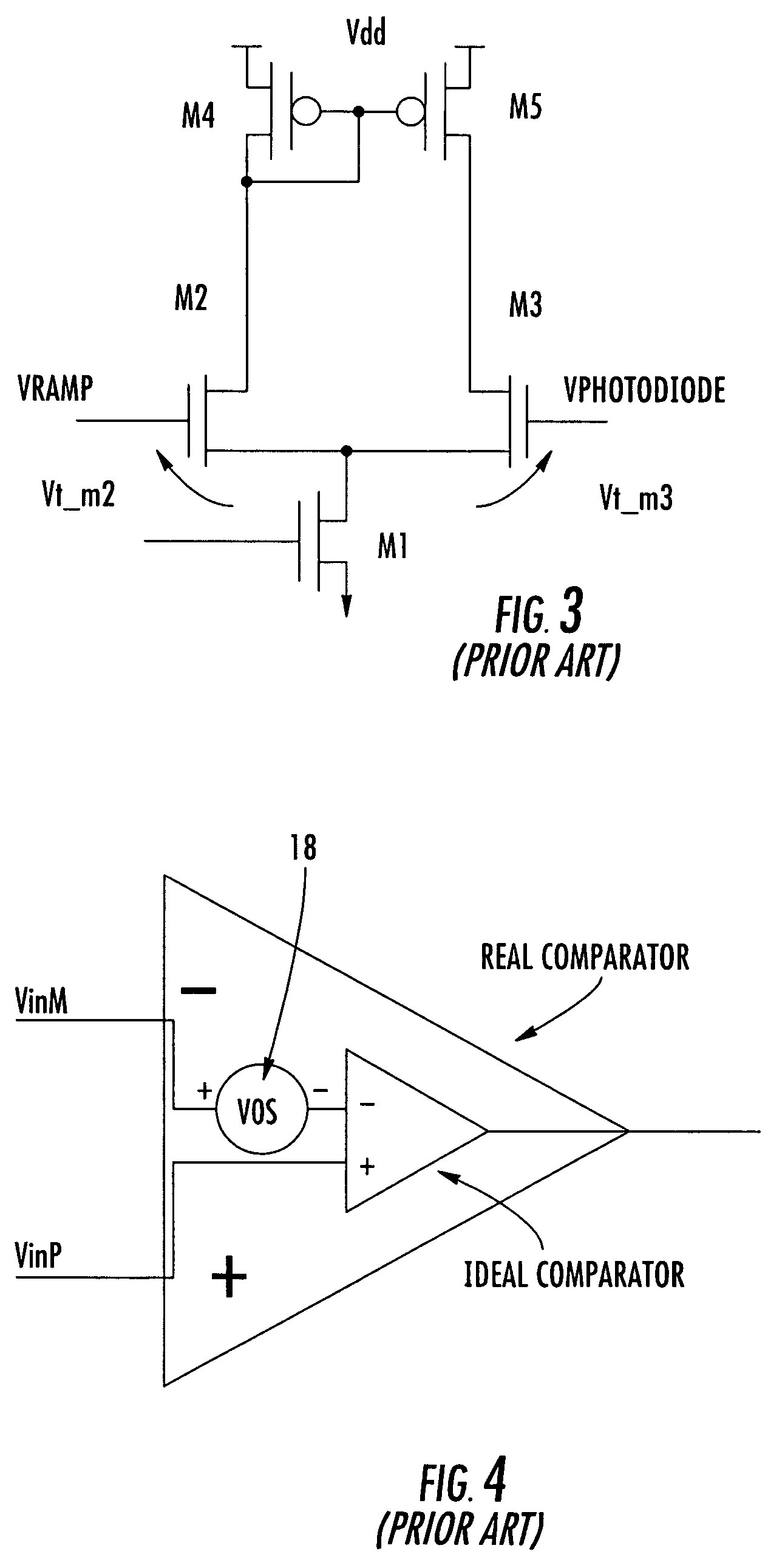
FIELD OF THE INVENTION[0001]The present invention relates to image sensors, and in particular, to a method for canceling offset noise of pixels in an image sensor, and to an image sensor operating according to the method.BACKGROUND OF THE INVENTION[0002]FIG. 1 shows the typical architecture of a digital pixel sensor. There is an ADC in each pixel 10 and a memory 12 external to the image plane which stores the image data. The common architecture includes a comparator 14 inside each pixel 10. One input to the comparator 14 is the photodiode voltage, the other input is a reference line Vramp 16 common to all the pixels 10.[0003]The rate of change of the voltage on the photodiode is proportional to the amount of light impinging on the pixel. On a graph of voltage against time, an increase in incident light will result in a steeper slope. By measuring the time it takes for a given swing (ΔV) on the pixel, the amount of light can be determined. This is illustrated in FIG. 2.[0004]FIG. 3 s...

Claims


Application Information

Patent Timeline
Patent Type & Authority Patents(United States)
IPC IPC(8): H04N3/14H04N5/335H04N5/357H04N5/365H04N5/3745
CPCH04N5/3575H04N5/3655H04N5/37455H04N25/616H04N25/673H04N25/772
Inventor RAYNOR, JEFFREY
Owner STMICROELECTRONICS (RES & DEV) LTD
Why Eureka
Try Eureka